Chapter 9
Analyzing Single-Loop Negative Feedback Circuits
Gordon W. Roberts
Department of Electrical & Computer Engineering, McGill University
With the introduction of radio communications by Nikola Tesla followed by its commercialization by Guglielmo Marconi, the need for circuits that oscillate was instrumental for their operation. Circuit designers eventually discovered a method to create oscillator circuits by feeding back a portion of the output signal from an amplifier to its input and having it constructively interfere with it to provide at its output a fixed-amplitude periodic signal. The circuit principle became known as positive feedback. In 1927 Harold Black proposed an alternative idea for the design of amplifier circuits. His idea was to feedback a portion of the output signal so that it subtracts from the input signal in a destructive manner. On doing so, the output signal would retain the shape of the input signal, with a higher magnitude, quite independent of the properties of the amplifier circuit. He referred to his circuit principle as one that uses negative feedback. While not immediately recognized, negative feedback is probably the most significance engineering discovery, as it is widely used across all disciplines of engineering in the realization of robust systems.
In this chapter, a very different approach to understanding circuit operation will be presented. It is based on a single-loop negative feedback perspective involving two parameters A and 𝛃 introduced by Black. The significance of this perspective was solidified with the stability theory of Harry Nyquist in 1932. Nyquist was able to identify the stability properties of circuit from the frequency behavior of the product A×𝛃. This help to explain the undesirable behavior of circuits that would sometimes “sing” or self-oscillate when employing negative feedback. Sometime later, Hendrik Bode in 1940 provided a simplified view of the theory of Nyquist where he introduced the idea of Bode plots: magnitude versus frequency and phase versus frequency plots. Further, he limited the discussion to one where the term A×𝛃 has no poles in the right-half plane and introduced the idea of phase and gain margin as measures of stability. Further, Bode demonstrated a relationship between phase margin and the dynamic behavior of a closed-loop circuit. Together, these insights were enough to trigger a revolution in the application of negative feedback across various engineering disciplines.
Using LTSpice to calculate several ratios of circuit variables, e.g., output voltage / branch current, it will be shown in this chapter how to extract the single-loop feedback parameters A and 𝛃 so that the loop transmission A × 𝛃 can be found. The method does not involve breaking any loop nor altering the bias conditions of the circuit, nor injecting signals inside the loop. Instead, it identifies the all the feedback parameters through an AC signal excitation at its input.
|
|
|
Fig. 9.1: The general form of a negative feedback structure as first proposed by H. Black. |

9.1 The Single-Loop Negative Feedback Structure
The basic structure of a system including some form of negative feedback as proposed by Black is shown in block diagram form in Fig. 9.1. The input signal is defined by the variable xs(s) and the output signal as xo(s). Here the block depicted by A(s) represents the feedforward gain stage of the closed-loop system, and the block denoted by 𝛃(s) represents the feedback block. It is assumed that the signal propagates in the direction of the arrows through these building blocks, i.e., they are unilateral. There is no signal that propagates back through the block. The summing node is used to subtract the feedback signal (xFdbk(s)) that is fed back from the output signal from the input signal xs(s) to create what is known as the error signal xErr(s), i.e.,
|
|
|
(9.1) |
Equation (9.1) is the central equation that all single-loop negative feedback circuits must implement. A circuit which does not implement this equation could not be classified as a single-loop negative feedback circuit.
Both A(s) and 𝛃(s) can be expressed in terms of these intermediate signals, xErr(s) and xFdbk(s), together with the output variable xo(s). For instance, the feedforward block A(s) can be defined as
|
|
|
(9.2) |
and the feedback block 𝛃(s) can be written as
|
|
|
(9.3) |
Consequently, Eqn. (9.1) can be re-written in terms of the feedback block 𝛃(s) as
|
|
|
(9.4) |
Substituting Eqns. (9.4) into (9.2), one can write the input-output transfer function Af(s) of the overall closed-loop system as
|
|
|
(9.5) |
|
|
|
Fig. 9.2: The four noncompliant single-loop feedback topologies incorporated with circuits: (a) voltage-mixing/voltage-sensing, (b) voltage-mixing/current-sensing, (c) current-mixing/voltage-sensing, and (d) current-mixing/current-sensing.
|

9.2 The Four Basic Feedback Amplifier Topologies
Amplifiers incorporating a single-loop negative feedback can be divided into four general classes depending on the nature of the sensing signal (i.e., voltage or current) and how the feedback signal combines or mixes with the input signal. The four general classes are described as follows:
|
(1) Voltage-Mixing/Voltage-Sensing (2) Voltage-Mixing/Current-Sensing (3) Current-Mixing/Voltage-Sensing (4) Current-Mixing/Current-Sensing. |
Figure 9.2 illustrates the four circuit topologies that are used to realize a single-loop negative-feedback circuit. Figure 9.2(a) illustrates the voltage-mixing/voltage-sensing topology where the input and output signals are vs and vo. As the input voltage signal is connected in series with the input to the amplifier and the output signal from the feedback network the front-end portion of this topology is said to implement a voltage-mixing, or series connection. At the output, the amplifier generates a voltage signal vo and this signal is “sensed” by the feedback amplifier to generate the feedback signal. Thus, the overall topology is referred to as voltage-mixing/voltage sensing arrangement. A second topology is shown in Fig. 9.2(b). This topology has the same front-end arrangement where the input signal is connected in series with the input to the amplifier and the output of the feedback circuit. As the output is a current signal io, and it is this signal that is “sensed” by the feedback network, this topology is referred to as a voltage-mixing/current-sensing arrangement.
In contrast, the two topologies of Fig. 9.2(c) and 9.2(d) use a current source as excitation and have the amplifier input placed in parallel with the output of the feedback network. One refers to this arrangement as a current-mixing one. In the case of the topology shown in Fig. 9.2(c), the output signal is a current signal. Thus, the feedback network “senses” the output current. Thus, the topology of Fig. 9.2(c) is said to be a current-mixing/current-sensing arrangement. Finally, the topology of Fig. 9.2(d) generates a voltage as its output signal and the feedback network senses this quantity. Consequently, the topology of Fig. 9.2(d) is called a current-mixing/voltage-sensing arrangement.
|
|
|
Fig. 9.3: Highlighting problem with voltage and current mixing when a source resistance is present. (a) voltage mixing, and (b) current mixing.
|

9.2.1 Input Signal Mixing Compliance
The four topologies of Fig. 9.2 have an important limitation when it comes to realizing the single-loop negative feedback structure of Fig. 9.1. To understand this, consider the voltage-mixing arrangement shown in Fig. 9.3(a). If one assumes the signal fed back by the feedback network is the signal vFdbk and the signal driving the amplifier is vErr, then according to KVL around the loop formed at the input, one can write
|
|
|
(9.6) |
If one assumes a one-to-one correspondence between the signals of the topology of Fig. 9.3(a) and that of the feedback structure of Black shown in Fig. 9.1, one can write:
|
|
|
(9.7) |

The voltage variable vRs is clearly not account for in the Black's theory. Thus, the error signals defined by Eqn. (9.1) and (9.6) are different. The topology of Fig. 9.3(a) is not compliant with the mixing arrangement proposed by Black.
Likewise, a similar result occurs with the current-mixing topology highlighted in Fig. 9.3(b). Here, one can use KCL and relate the current signals at the input port of the amplifier as
|
|
|
(9.8) |
Assuming the following one-to-one correspondence between Fig. 9.1 and Fig. 9.3(b), one can claim
|
|
|
(9.9) |

and conclude that the current variable iRs is not accounted for by Black's theory. Thus, the error signals defined by Eqn. (9.1) and (9.8) are different. The topology of Fig. 9.3(b) is not input compliant with the structure proposed by Black.
|
|
|
Fig. 9.4: Three equivalent voltage-mixing arrangements; two are compliant with Black’s single-loop feedback structure: (a) noncompliant, (b) compliant, and (c) compliant. |

|
|
|
Fig. 9.5: Three equivalent current-mixing arrangements; two are compliant with Black’s single-loop feedback structure: (a) noncompliant, (b) compliant, and (c) compliant. |

Fortunately, there is a simple topological fix that can be used to ensure a single-loop negative feedback circuit is compliant with the structure of Black. By associating the source resistance Rs with either the basic amplifier or the feedback network, the feedback circuit can be made compliant with the feedback structure of Black while maintain circuit equivalence. These situations are depicted in Figs. 9.4 and 9.5 for the voltage and current mixing arrangements. As is evident from these two figures, feedback compliance comes down to selecting the error and feedback signals appropriately. More on this in the next section.
|
|
|
Fig. 9.6: Highlighting the physical difference between an output signal from a circuit with a feedback loop and the signal being sensed by the feedback network. (a) The output voltage is the same signal that is being sensed by the feedback network, and (b) The output voltage is different from the current signal that is being sensed by the feedback network. |

|
(a)
(b)
|
|
Fig. 9.7: Highlighting the difference between a sense and output signal: (a) Relabelling the output variable of the single-loop feedback structure of Black as the sense variable xSen. (b) Including a 𝛾(s)-block that relates the sense variable xSen to the designated output signal xo. |


9.2.2 Output Signal Sensing Compliance
Voltage or current sensing refers to the signal that is being sensed and fed back to the mixing element through the feedback network. The circuit variable which the circuit senses is either a node voltage or branch current, as the choice is somewhat arbitrary. However, it is paramount that the sense variable is located directly on the circuit path of the feedback loop as either a node voltage or branch current. Any circuit variable not on the path of the feedback loop cannot be sensed and be used to provide corrective action. In many circumstances, the sense variable is not equal to the designated output. For instance, in Fig. 9.6(a) the output of the circuit with a feedback loop is designated as the output voltage vo. As the feedback network is connected in parallel with the amplifier output, the sense signal is the voltage developed across the load resistor RL; this is also designated as the output voltage vo. The arrangement shown in Fig. 9.6(a) would therefore be sense compliant with what Black intended. In the situation depicted in Fig. 9.6(b), the output of the circuit is again designated as the voltage across the load RL, however, the feedback network is connected in series with the load resistor and will be sensing the load current iL instead. Consequently, according to Black’s theory, the sense variable should be designated as the load current. In other words, the arrangement of Fig. 9.6(b) would not be sense compliant with Black’s intention. To avoid any future confusion, we will designate the output variable of the feedback topology proposed by Black as the sense variable and designate it as xSen(s). As this signal may be different from the output designated signal variable, an additional block denoted by 𝛾(s) is included, as shown in Fig. 9.7. Consequently, the input–output transfer function Af(s) of the overall feedback structure of Black’s model with the 𝛾-block included would be defined as:
|
|
|
(9.10) |
The burden of assignment of which variable should act as the sense signal and which is the output is always left to the person undertaking the feedback analysis.
9.3 Feedback Parameter Isolation Method Using the Intermediate Transfer Function (IF) Approach
In this section, a method of identifying the feedback parameters A(s) and 𝛃(s) will be described based on the application of a set of transfer functions defined from the input to the intermediate variables of the feedback circuit, such as xErr(s), xFdbk(s) and xSen(s). Consequently, these transfer functions will be referred to as the intermediate transfer functions, or IFs for short.
According to the block diagram of Fig. 9.7(a) or (b), the A(s) and 𝛃(s) blocks can be defined as the ratio of two signal variables as:
|
|
|
(9.11) |
and
|
|
|
(9.12) |
Finally, the 𝛾-block of Fig. 9.7(b) can be defined as
|
|
|
(9.13) |
It is interesting to note that the loop transmission Ab(s) is simply the ratio of the feedback signal and the error signal, or expressed as the ratio of xFdbk(s) to xErr(s), as
|
|
|
(9.14) |
|
|
|
Fig. 9.8: Illustrating the intermediate transfer functions associated with a single-loop feedback circuit. |

To understand the physical significance of the ratio of these feedback variables, consider the transfer functions from the input forcing function (V or I) to the intermediate variables associated with the single-loop feedback structure. Rather than track all possible variables, we’ll use x with a subscript to represent the circuit variable of interest to stay as general as possible. There are three circuit variables that we mention in the description of the single-loop feedback structure. Specifically, xFdbk(s), xErr(s), and xSen(s). However, xErr(s) is a dependent on the difference between xs(s) and xFdbk(s), thus only two transfer functions are necessary to complete this analysis. These are:
|
|
|
(9.13) |
and
|
|
|
(9.14) |
The transfer function from the input to the error signal can be defined as
|
|
|
(9.15) |
Figure 9.8 depicts the IFs, TFdbk(s), TErr(s) and TSen(s), as superimposed on single-loop feedback structure. Using the above IFs, the feedback components, A(s) and 𝛃(s), can then be expressed as follows:
|
|
|
(9.16) |
and
|
|
|
(9.17) |
As the product of A(s) × 𝝱(s) is central to our feedback invertigation, the general form of this product can be expressed as
|
|
|
(9.18) |
Finally, the 𝛾-block can be identified as
|
|
|
(9.19) |
where To(s) is the input-output transfer function, i.e.,
|
|
|
(9.20) |
|
(a)
|
(b)
|
|
Fig. 9.9: An example of a voltage-mixing/voltage-sensing feedback amplifier. (a) Noninverting op-amp configuration with source resistance included. The feedback error signal is identified in terms of the input signal and the designated feedback signal. (b) The small-signal equivalent circuit of the noninverting configuration captured in LTSpice. The critical signal nodes that are involved in the feedback component parameters extraction are highlighted in yellow.
|
|


9.3.1 Voltage-Mixing/Voltage-Sensing Topology
As the first example of this chapter, we present in Fig. 9.9(a) an op-amp connected in the noninverting configuration with a gain of 11 V/V and driven by a source with a 10 kΩ resistance. This amplifier is an example of a voltage-mixing/voltage-sensing feedback arrangement. The voltage amplifier is to be assumed to have a 1 kHz single-pole response with a DC gain of 100,000 V/V. (This corresponds to an amplifier with a unity gain frequency of 100 MHz). Moreover, the amplifier has an input differential resistance of 100 kΩ and an output resistance of 10 Ω. We would like to analyze this feedback amplifier and identify the feedback parameters (A, 𝛃 and 𝛄) using the parameter isolation method described above.
To begin, the circuit was entered into LTSpice and the schematic is displayed
in Fig. 9.9(a). Critical to applying the parameter isolation method to a voltage-mixing/voltage-sensing
feedback arrangement is the need to identify the location of the feedback and
sensing signals. As the output voltage is sensed directly by the feedback
network, the 𝛾-block
is equal to unity. To keep track of this fact, the output node voltage will be
labeled as SEN_OUT. As the sense-to-mixing-element feedback path
involves R2, the feedback signal vFdbk
would appear at the left-side node of R2 as shown in Fig. 9.9(a). In
the LTSpice circuit description of Fig. 9.9(b), this same node will be labelled
as Fdbk. As well, the input voltage will be labelled as IN. By
definition, the error signal vErr is the difference
between the input voltage and the feedback signal, as highlighted in Fig.
9.9(a). As this error signal includes the source resistance Rs
within the amplifier circuit, the circuit of Fig. 9.9 is compliant with Black’s
topology.
|
|
Fig. 9.10: The A and 𝛽 parameters of the noninverting amplifier of Fig. 9.9.
|

To obtain the IFs TFdbk(j𝜔) and TSen(j𝜔), an AC analysis of the circuit of Fig. 9.9(b) is to be performed over a bandwidth from 1 Hz to 100 MHz. The input source was assigned a 1-V, 0-degree AC signal level and the following Spice directive was included on the LTSpice schematic:
.AC DEC 10 1Hz 100MegHz
The analysis was run, and the waveform viewer appears. With a 1-V AC signal, TFdbk(j𝜔) and TSen(j𝜔) are equivalent to the two voltage signals stored in the waveform viewer, V(FDBK) and V(SEN_OUT). The input-output transfer function To(j𝜔) would simply be obtain using the voltage signal V(OUT). Consequently, the A and 𝛃 would be computed and displayed using the following two viewer commands:
|
|
|
(9.21) |
and
|
|
|
(9.22) |
As previously mentioned, 𝛄 is equal to unity. To compare the actual input-output transfer function V(OUT) to that computed by feedback theory, i.e., Eqn. (9.10), one can write
|
|
|
(9.23) |

The AC results corresponding to A, 𝛃 and Af, the three above mentioned components computed by LTSpice are shown in Fig. 9.10. As is evident from this figure, at very low frequency the A block has a gain of 100 dB or 105 V/V, a unity gain frequency of 100 MHz. The feedback factor 𝛃 is equal to 0.0909 V/V from 1 Hz to 10 MHz but starts to increase above this frequency. The closed-loop gain predicted by Eqn. (9.23) is plotted in the top window pane and compared to that computed directly by LTSpice. They clearly agree, as they both have a low-frequency gain of 11 V/V with a 3-dB bandwidth of approximately 1 MHz.
|
(a)
|
(b)
|
Fig. 9.11: (a) Noninverting amplifier (duplicate of Fig. 9.9(b). (b) Comparing the open-loop amplifier behavior with different closed-loop behavior set by stepping through the feedback resistor R2 values: 1k, 10K, 100k and 1000k Ω. The trade-off between closed-loop gain and bandwidth is clearly evident.
|
|

To illustrate that the flexibility of the parameter isolation method, let us compare the open-loop response with the closed-loop input-output response for different feedback resistor R2 values having the following values: 1k, 10k, 100k and 1000 kΩ. This is achieved by setting the value of R2 to a parameter {R2_value} and including the following Spice directive .STEP command:
.STEP param R2_value LIST 1k 10k 100k 1000k
The circuit arrangement of Fig. 9.9(b) will be used. The LTSpice analysis is then repeated, and the AC response results are shown in Fig. 9.1(b). As is clearly evident, the open-loop response displays a trade-off between gain and bandwidth. More precisely, one can expresses this as
|
|
fT (Hz) = Gain (V/V) x Bandwidth (Hz)
|
(9.24) |
where fT is frequency in Hz where the magnitude response crosses the 0-dB axis.
|
(a)
|
(b)
|
|
(c)
|
|
|
Fig. 9.12: A broadband amplifier composed of a feedback triple. The biasing circuitry is not shown as we are only concerned with small-signal equivalent circuit representation that will be given shortly. (a) The output voltage signal is outside the feedback loop created by resistor RF , so it cannot be used to identify the feedback parameters. (b) A sense current ISen is identified inside the feedback loop. (c) Small signal circuit representation with sense and output signals identified. As well as the reference and feedback signals. |
|


|
|
|
Fig. 9.13: The small-signal equivalent circuit of the feedback triple using voltage-mixing shown in Fig. 9.12 as captured in LTSpice. An AC Spice directive is included. As well, the voltage-mixing feedback node labels IN and Fdbk are highlighted in yellow. Also highlighted in yellow is the sense current ISen and the output node voltage. The sense current will be derived from the zero-valued voltage source identified as VSen using the waveform viewer in LTSpice.
|

9.3.2 Voltage-Mixing/Current-Sensing Topology
The next example, shown in Fig. 9.12(a), illustrates a cascade of three transistors in a voltage-mixing/current-sensing feedback configuration known as a feedback triple. Unfortunately, the output voltage signal is not inside the feedback loop form by RF. Thus, to identify the parameters of the feedback amplifier, a sense signal within the feedback loop is required. Such a current signal has been designated in Fig. 9.10(b). While the biasing information is not included in either Fig. 9.10(a) or (b), the small-signal parameters of each transistor is given below:
|
Q1 @ IC=0.6 mA: rp1=4.167 kΩ, gm1=24 mA/V Q2 @ IC=1.0 mA: rp2=2.5 kΩ, gm2=40 mA/V Q3 @ IC=4.0 mA: rp3=625 kΩ, gm3=160 mA/V
|
Using the above information, we can replace each transistor in Fig. 9.12(b) by its small-signal equivalent circuit as shown in Fig. 9.12(c). This circuit was then captured by LTSpice as shown in Fig. 9.13. An AC Spice directive is included. As well, the voltage-mixing feedback node labels IN and FDBK are highlighted in yellow. Also highlighted is the sense current with ISEN and the output voltage as OUT. The sense current will be derived from the zero-valued voltage source identified as Vsen using the waveform viewer in LTSpice. Notice that the input node corresponds with the IN labeled node. According to the voltage-mixing principles described above, the feedback parameters (A, 𝛃 and 𝛄) can be identified using the following intermediate transfer function ratios:
|
|
|
(9.25) |
|
|
|
(9.26)
|
and
|
|
|
(9.27) |
|
|
|
Fig. 9.14: The A, 𝛃 and 𝛄 parameters of the feedback triple amplifier arrangement of Fig. 9.9.
|
Fig. 9.15: The closed-loop gain Af from input to output (vout/vs)
|


The AC results corresponding to A, 𝛃 and 𝛄 as computed by LTSpice are shown in Fig. 9.14. As is evident from these results, they are all frequency independent. This should not be surprising, as no capacitors appear in the small-signal circuit of Fig. 9.13. The A parameter is found to have a gain of about 65.31 A/V, the 𝛃 parameter a value of about 11.937 V/A and the 𝛄 parameter has a value of 594.05 V/A. As a check on these values, the overall closed loop gain Af can be derived from Eqn. (9.10) according to the following:
![]()
As illustrated in Fig. 9.15, the LTSpice results of the input-output behavior (V(OUT)/V(IN)) agree with this result.
|
(a)
|
(b) |
|
Fig. 9.16: A single-stage amplifier circuit using a current-mixing/voltage-sensing arrangement. (a) Noncompliant, and (b) Compliant arrangement by moving source resistance into A-block. |
|


|
|

9.3.3. Current-Mixing/Voltage-Sensing Topology
In Fig. 9.16(a) we display a single-stage common-emitter amplifier with feedback resistor Rf using a current-mixing/voltage-sense topology. Here the node designated as the output voltage is being sensed by the feedback network involving the feedback resistor Rf. It is desired to isolate the feedback parameters (A, 𝛃 and 𝛄) using the parameter isolation method described above. Critical to applying the parameter isolation method to a current-mixing feedback arrangement is the need to identify the current mixing node of this amplifier. In a single-loop feedback topology there is only one path interconnecting the output signal to the rest of the structure. Thus, resistor Rf in Fig. 9.16(a) takes on this role and carries the feedback current IFdbk to the current-mixing node. Thus, the non-output-connected terminal of Rf must be the mixing node. As the source resistance RS is found to the left of this node, the topology of Fig. 9.16(a) would be non-compliant. By moving the source resistance RS to the right of the mixing node as shown in Fig. 9.16(b), the circuit is now compliant with a current-mixing/voltage-sensing topology.
To capture the critical currents using LTSpice, three 0-valued voltages sources are connected in series in each branch as highlighted in Fig. 9.17. LTSpice allows direct access to the current flowing through these voltage sources. Also highlighted in yellow in this figure is the input current and the sense/output node signal. Here we use the notation SEN_OUT to signify its dual role, as both a sense signal and output signal. As such, 𝛄 is equal to unity. Using an AC analysis directive, the feedback parameters (A and 𝛃) would be defined according to the following:
|
|
|
(9.28) |
and
|
|
|
(9.29) |
|
|
Fig. 9.18: The closed-loop gain parameter Af and the open-loop parameters A and 𝛃 for the single-stage amplifier shown in Fig. 9.16. 𝛄 is equal to unity. |

The AC results computed by LTSpice are shown in Fig. 9.18. Here the transistors are modelled as the 2N3904 type. For frequencies below 10 kHz, the closed-loop amplifier has an input-output gain Af of 44.27 kV/A, the open-loop gain A is 821.7 kV/A and 𝛃 is 21.4 𝜇A/V. As established earlier, 𝛄 is equal to unity. As a quick check, using Eqn. (9.10), one finds the estimated overall closed loop gain as
![]()
which is essentially the same value found directly by LTSpice (Af = 44.27 kV/A); any differences are numerical issues related to the hand calculation.
|
(a)
|
(b) |
|
(c) |
(d) |
|
Fig. 9.19: Preparing a current-mixing/current-sensing feedback circuit for analysis: (a) Identifying the feedback loop, (b) As the output voltage is outside the feedback loop of the amplifier, a sensing current has been identified that is inside the loop, (c) Replacing the input voltage source and its source resistance by its Norton’s equivalence, and (d) A fully compliant circuit arrangement that meets the definition of a current-mixing/current-sensing topology and is equivalent to the circuit of part (c). |
|


|
|
|
|
Fig. 9.20: The current-sensing shunt-feedback amplifier circuit of Fig. 9.19(c) as captured in LTSpice. An AC Spice directive is included. As well, the current-mixing branch currents are highlighted in yellow. Also highlighted is the 0-valued voltage source that measures the sense current ISen, the input current source and the output voltage signal.
|
Fig. 9.21: The closed-loop gain parameter Af and the open-loop parameters A, 𝛃 and 𝛄 for the amplifier shown in Fig. 9.20.
|


9.3.4 Current-Mixing/Current-Sensing Topology
As the final example of the four feedback amplifier topologies, a noncompliant current-mixing/current-sensing circuit is display in Fig. 9.19(a). Here the input and output are voltage signals. As the feedback loop is formed on the emitter side of Q1 and Q2, the output voltage signal is clearly outside the loop. Rather, the emitter current of Q2 is selected as the sense signal as it is inside the feedback loop (see Fig. 9.19(b)). The mixing node occurs at the base of Q1, as it is the point at which the feedback resistor Rf terminates on the input side of the amplifier. Unfortunately, there is no physical way the voltage at this node can be connected in series with the input voltage source. Rather, if the input voltage source and its source resistance is converted to its Norton’s equivalent (See Fig. 9.19(c)), then by moving the shunt source resistance Rs next to the amplifier input (Fig. 9.19(d)) the circuit is now fully compliant with a current-mixing/current-sensing topology. Note that the source resistance is AC coupled to the circuit to prevent it from altering the DC bias level of the amplifier.
A schematic of the circuit of Fig. 9.19(d) captured by LTSpice is shown in Fig. 9.20. Here, transistors Q1 and Q2 are modelled after commercial npn transistors of the 2N3904 type taken from the LTSpice library of active components. The three mixing currents can be made accessible using the three 0-valued voltage sources shown in the figure. Once again, these mixing currents are highlighted in yellow. Also, the sensing current, input current and the output voltage are highlighted in yellow as well. Using an AC analysis directive, the feedback parameters (A, 𝛃 and 𝛄) can be identified using the following input-output and intermediate transfer function ratios:
|
|
|
(9.30) |
|
|
|
(9.31) |
and
|
|
|
(9.32) |
The AC results computed by LTSpice are shown in Fig. 9.21. As is evident from this figure, at low frequency (below 10 kHz) the closed-loop amplifier has an input-output gain Af of 3.45 kV/A, the open-loop gain A is 341.9 A/A, 𝛃 is 254.3 mA/A and 𝛄 is 886.1 V/A. As a quick check, using Eqn. (9.10), one finds
|
|
|
|
which is very similar to the value found directly by LTSpice (Af = 3.45 kV/A). While here we looked at low frequencies parameters, the results are true for all frequencies.
This concludes our discussion of the feedback parameter isolation method. The method was applied to examples of the four general topologies and all four were shown to give consistent results.
9.4 Input and Output Resistance Impacted by Feedback
An important attribute of negative feedback is its effect on the input and output resistances of the open loop amplifier. This section will describe these effects.
9.4.1 Input Resistance
The input resistance of a voltage-mixing feedback arrangement will be described below. This will be followed by a description of the input resistance of a current mixing feedback arrangement.
Voltage-Mixing Feedback Arrangement:
To see how feedback affects the input resistance (impedance) of a voltage-mixing feedback arrangement, recall KCL around the front-end loop of the circuit, such as that shown on the middle row of Table 9.1, is simply
|
|
|
(9.33) |
However, in general terms, according to Eqn. (9.18) one can related the feedback signal to the error signal as
|
|
|
(9.34) |
Consequently, substituting Eqn. (9.34) into (9.33) results in
|
|
|
(9.35) |
Dividing
both sides of this equation by the source current ![]() ,
,
|
|
|
(9.36) |
leads to an expression whose terms on the right- and left-hand side has dimensionally of ohms. It is obvious that the resistance seen looking into the input port of the closed-loop amplifier is
|
|
|
(9.37) |
Less
obvious is the fact the resistance seen looking into the port defined by the
error signal, ![]() ,
would be defined as the ratio of
,
would be defined as the ratio of ![]() ,
and would equal the sum of the source resistance
,
and would equal the sum of the source resistance ![]() and
resistance seen looking into the input port of the basic amplifier
and
resistance seen looking into the input port of the basic amplifier ![]() ,
i.e.
,
i.e.
|
|
|
(9.38) |
Consequently, substituting Eqns. (9.37) and (9.38) into Eqn. (9.36) leads to
|
|
|
(9.39) |
Here
one can see that the input resistance to the closed-loop amplifier is ![]() times
greater than the sum of the source resistance and input resistance of the
open-loop amplifier. It is important to note here that the input resistance to
the basic amplifier
times
greater than the sum of the source resistance and input resistance of the
open-loop amplifier. It is important to note here that the input resistance to
the basic amplifier ![]() is
the same regardless of whether the amplifier is configured in open- or
closed-loop. This is not true for all ports of a closed-loop arrangement,
though. For instance, following the above development, one can show that
is
the same regardless of whether the amplifier is configured in open- or
closed-loop. This is not true for all ports of a closed-loop arrangement,
though. For instance, following the above development, one can show that
|
|
|
(9.40) |
Consequently,
defining ![]() as
the resistance seen looking into the output port of the feedback network,
suggests
as
the resistance seen looking into the output port of the feedback network,
suggests
|
|
|
(9.41) |
It
is important to note here that the port resistance ![]() is
not equal to the resistance seen looking into the output port of the feedback
network in open loop.
is
not equal to the resistance seen looking into the output port of the feedback
network in open loop.
|
|
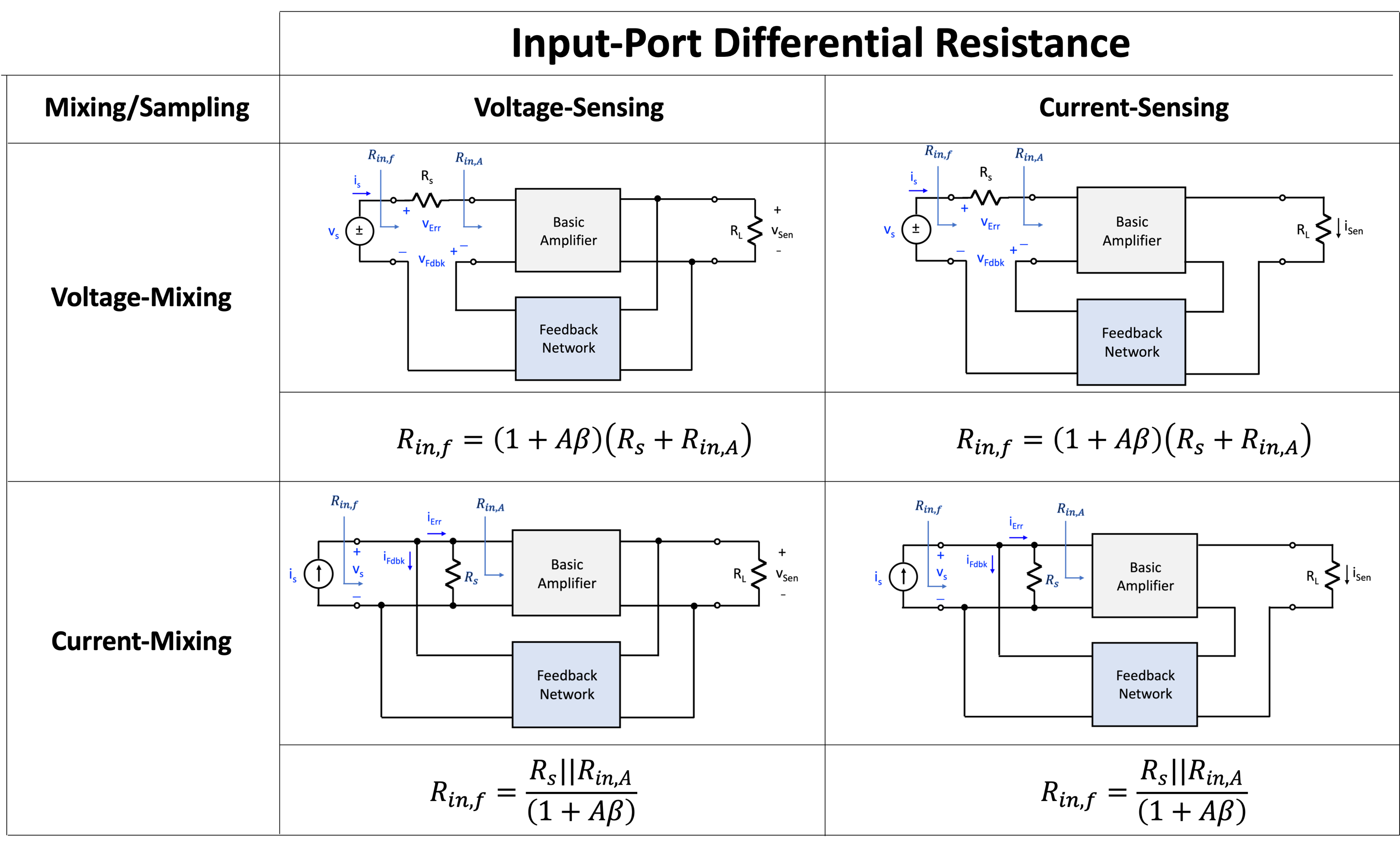
Current-Mixing Feedback Arrangement:
In much the same manner, the input conductance (admittance) of a current mixing feedback arrangement, such as that shown in the bottom row of Table 9.1, can be described as
|
|
|
(9.42) |
To see this, consider applying KCL at the mixing node of the feedback circuit, leading one to write
|
|
|
(9.43) |
As ![]() , one can write
, one can write
|
|
|
(9.44) |
As
the voltage at the mixing node ![]() is
common to the input port of the closed-loop amplifier and the input port of the
open-loop amplifier, one can divide both the right- and left-hand side of Eqn.
(9.44) to obtain
is
common to the input port of the closed-loop amplifier and the input port of the
open-loop amplifier, one can divide both the right- and left-hand side of Eqn.
(9.44) to obtain
|
|
|
(9.45) |
As
|
|
|
(9.46) |
On substituting Eqns. (9.46) into (9.45), Eqn. (9.42) results. One often finds this expression written in terms of resistances rather than conductance’s as follows
|
|
|
(9.47) |
where
|
|
|
(9.48) |
Table 9.1 summaries these two results as it applies to the four general mixing and sensing arrangements.
|
(a)
|
(b) |
|
Fig. 9.22: Computing
the input resistance of the noninverting amplifier circuit of Fig. 9.9: (a) LTSpice
circuit setup, and (b) frequency plot of the various port resistances, |
|


Example:
To confirm our premise, let us return to the voltage-sensing series mixing circuit of Fig. 9.9 involving the operational amplifier and calculate the input resistance with and without feedback. The LTSpice test setup is shown in Fig. 9.22(a). Using an AC analysis request, the resistances seen looking into the input port of the closed-loop configuration, input port to the basic amplifier, and the output port of feedback network can be found. The results are shown in Fig. 9.22(b). Through the application of the cursor facility of the waveform viewer, one sees that the input resistance at a frequency of 10 Hz is 908.3 MΩ for the closed-loop circuit. According to the parameter isolation method, one previously found A = 105 V/V and 𝛽 = 0.09 V/V. As Rin,A = 100 kΩ and Rs=10 kΩ, feedback theory suggests Rin,f = (1 + A𝛽) × (Rin,A+Rs) = (1 + 105 × 0.09) (100kΩ|+10kΩ) = 990.1 MΩ. This value is quite close to the value obtain through LTSpice. Likewise, one sees that that the resistance seen looking into the input port to the basic amplifier as computed by LTSpice is exactly equal to the sum of Rs and Rin,d of 110 kΩ. One also should note that the output resistance of the feedback network in open loop is expected to be in the neighbourhood of 1 kΩ; however, the LTSpice analysis reveals the resistance seen looking into the output port of the feedback network Ro,𝛽 in a closed-loop arrangement is very high at 908.2 MΩ. This agrees with the theory captured the expression derived in Eqn. (9.41).
9.4.2 Output Resistance
The
output resistance seen looking into the sense port of a feedback circuit can be
expressed in terms of its loop gain and circuit parameters. However, unlike
the previous expressions for the input resistance, the output resistance expression
involves a different loop gain parameter than that which was used previously.
More specifically, the expressions will be written in terms of the no-load
loop gain, denoted here as ![]() as
opposed to the previously used loaded loop gain expression
as
opposed to the previously used loaded loop gain expression ![]() .
.
The following will address the output conductance of a feedback arrangement that uses voltage sensing. Following this, the output resistance of a feedback arrangement that uses current sensing will be described.
|
|
|
Fig. 9.23: Simplified representation of a voltage-mixing topology with different sensing arrangements: (a) voltage sensing, and (b) current sensing. |
|


Voltage Sensing Arrangement:
Consider
the simplified representation of a voltage-mixing, voltage-sensing feedback
arrangement with load RL shown in Fig. 9.23(a). Here the basic
amplifier is represented as a 2-port network and a voltage gain ![]() and
output resistances Ro,A. Likewise, the feedback network is
represented as a 2-port network with voltage gain
and
output resistances Ro,A. Likewise, the feedback network is
represented as a 2-port network with voltage gain ![]() and
output resistance Ro,𝛽.
Both networks are assumed to have infinite input resistance. Using the feedback
parameter isolation method of Section 9.3, the two feedback parameters A
and 𝛽 can be
found to be
and
output resistance Ro,𝛽.
Both networks are assumed to have infinite input resistance. Using the feedback
parameter isolation method of Section 9.3, the two feedback parameters A
and 𝛽 can be
found to be
|
|
|
(9.49) |
and
|
|
|
(9.50) |
Consequently, the closed-loop input-output gain can be stated as
|
|
|
(9.51) |

Using the voltage-divider principle for establishing the output resistance of a circuit, consider the value of RL that forces the closed-loop gain to reduce to 1/2 from its no-load condition. As the no-load closed-loop gain condition occurs when RL=∞, one can state the output resistance of the closed-loop amplifier Ro,f as solution to the equation,
|
|
|
(9.52) |

On substituting Eqn. (9.51), one can write
|
|
|
(9.53) |

Solving for Ro,f, one would find
|
|
|
(9.54) |
Here
it is evident that the output resistance of the open-loop amplifier is reduced
by the term ![]() As
As
![]() and
and
![]() represent
the no-load feedback parameters, i.e.,
represent
the no-load feedback parameters, i.e.,
|
|
|
(9.55) |
and
|
|
|
(9.56) |
One can state more generally, without imposing limitations on the nature of the circuit that the output resistance of the closed loop amplifier would be described in terms of the output resistance of the basic amplifier as
|
|
|
(9.57) |
|
|

Current Sensing Arrangement:
Consider
the simplified representation of a voltage-mixing, current-sensing feedback
arrangement with load RL shown in Fig. 9.23(b). Here the basic
amplifier is represented as a 2-port network and a transconductance gain ![]() and
output resistances Ro,A. Likewise, the feedback network is
represented as a 2-port network with transresistance gain
and
output resistances Ro,A. Likewise, the feedback network is
represented as a 2-port network with transresistance gain ![]() and
output resistance Ro,𝛽.
The transconductance network is assumed to have infinite input resistance but
the input to the transresistance network is assumed to be a short circuit
between its input terminals. Using the feedback parameter isolation method of
Section 9.3, the two feedback parameters A and 𝛽 can be found to be
and
output resistance Ro,𝛽.
The transconductance network is assumed to have infinite input resistance but
the input to the transresistance network is assumed to be a short circuit
between its input terminals. Using the feedback parameter isolation method of
Section 9.3, the two feedback parameters A and 𝛽 can be found to be
|
|
|
(9.58) |
and
|
|
|
(9.59) |
The closed-loop input-output gain can then be stated as
|
|
|
(9.60) |

Using the current-divider principle for establishing the output resistance of a circuit, consider the value of RL that forces the closed-loop gain to reduce to 1/2 from its no-load condition. As the no-load closed-loop gain condition occurs when RL=0, one can state the output resistance of the closed-loop amplifier Ro,f as solution to the equation,
|
|
|
(9.61) |

Substituting Eqn. (9.60) into the above expression, and solve for Ro,f, one finds
|
|
|
(9.62) |
As both Go and Bo represents the no-load condition for each feedback parameters, the above result can be re-stated in terms of the no-load feedback parameters as
|
|
|
(9.63) |
Table 9.2 summaries these two results as it applies to the four general mixing and sensing arrangements.
|
(a)
|
(b) |
|
Fig. 9.24: LTSpice circuit capture for computing the
output conductance of the operational amplifier circuit of Fig. 9.9: (a)
LTSpice circuit setup, and (b) frequency plot of port resistances, |
|


Example:
To
confirm our premise, let us return to the voltage-sensing series mixing circuit
of Fig. 9.9 involving the operational amplifier and calculate the output
resistance with and without feedback. The LTSpice test setup is shown in Fig.
9.24(a). Here the input voltage source is set to zero and the output is driven
with an external AC voltage source Vt. Using an AC analysis request, the
resistances seen looking into the output port of the closed-loop configuration
and that of the basic amplifier can be found. The results are shown in Fig. 9.23(b).
Through the application of the cursor facility of the waveform viewer, one sees
that the output resistance at a frequency of 10 Hz is 1.1 mΩ for the
closed-loop circuit. Likewise, one sees that that the resistance seen looking
into the input port to the basic amplifier as computed by LTSpice is exactly
equal to the Ro,A of 10 Ω. According to the parameter
isolation method, as the previous computed ![]() and
and
![]() was
performed under no-load conditions (Section 9.3.1), thus
was
performed under no-load conditions (Section 9.3.1), thus ![]() =
105 V/V and
=
105 V/V and ![]() =
0.09 V/V. As Ro,A = 10 Ω, feedback theory suggests
=
0.09 V/V. As Ro,A = 10 Ω, feedback theory suggests ![]() .
This value is the same as the value obtain through LTSpice.
.
This value is the same as the value obtain through LTSpice.
9.5 Stability Behavior of Single-Loop Feedback Circuits Described by Black
In this section, the stability behavior of a circuit based on the feedback parameters A and 𝛃 identified by Black will be described.
9.5.1 Loop Transmission A𝛃(s)
The closed-loop transfer function of a single-loop feedback structure with 𝛾-block shown in Fig. 9.7(b) has already been described as
|
|
|
(9.64) |
Assuming there are no pole-zero cancelation between the numerator and denominator terms of Af(s), then the poles of this transfer function are the roots of the expression,
|
|
|
(9.65) |
While mathematically possible, one can contrive a transfer function for the 𝛾-block where one of its zeros can cancel with one of the zeros of 1+ A(s)𝛃(s). However, in practise, this situation is rare and will be ignored going forward.
At the core of this expression is the term A(s)𝛃(s). Because of its importance to the dynamic operation of a closed-loop system it is commonly referred to as the loop transmission, denoted here as
|
|
|
(9.66) |
|
(a)
|
(b) |
|
Fig. 9.25: Illustrating Cauchy principle of argument theorem of complex functions: (a) Poles and zeros enclosed by arbitrary contour 𝞒 in the s-plane. and (b) illustrating the complete phase change of f(s) as it is evaluated at all points defined by the contour 𝞒 (s0, s1, s2, …). |
|


9.5.2 Nyquist Stability Criterion
The stability behavior of a closed-loop single-loop feedback system can be deduced from the frequency behavior of its loop transmission, A𝛃(s), and knowledge of location of the poles of A𝛃(s) – said to be the stability of the open-loop system. This statement was first made by Nyquist back in 1932 and had a profound effect on the development of electronics and control systems. Bode went one step further and assumed that the stability behavior of the open-loop system was stable and thus was able to replace the Nyquist statement with two, although equivalent, point metrics of stability, called gain and phase margin. Due to the simplicity of Bode’s statement, the application of feedback in circuits and systems flourished. In this subsection, the stability statement of Nyquist and Bode will be described.
At the core of Nyquist’s statement is Cauchy’s principle of argument theorem for complex functions. A complex function f(s) that is analytic inside some contour 𝚪 that encloses a finite number of poles and zeros inside the region bounded by this contour, see Fig. 9.25(a), will satisfy the following integral equation:
|
|
|
(9.67) |
As the number of zeros and poles of f(s) are countable
by integer numbers, the integration will always sum to some integer multiple of
2𝜋. This can be interpreted to represent the total phase change
of a vector pinned at the origin of the complex s-plane as it rotates around a
new contour described by ![]() as depicted in Fig. 9.25(b). Another way of
expressing this statement is to count the number of times the phase vector
completes a phase change of 2𝜋, i.e.,
as depicted in Fig. 9.25(b). Another way of
expressing this statement is to count the number of times the phase vector
completes a phase change of 2𝜋, i.e.,
|
|
|
(9.68) |
The notation used here, specifically ![]() ,
is meant to be read as the number of times the phase vector centered at the
point 0+j0 completes a full 2𝜋 rotation,
or encirclement, as it moves along the contour described by the mapping
,
is meant to be read as the number of times the phase vector centered at the
point 0+j0 completes a full 2𝜋 rotation,
or encirclement, as it moves along the contour described by the mapping ![]() ;
the so-called Nyquist contour.
;
the so-called Nyquist contour.
As an example, if f(s) has no zeros or poles, or equal number of poles and zeros, enclosed with the contour 𝚪 then the number of encirclements is equal to zero. However, if there are 2 more zeros than poles bounded by the region defined by 𝚪 then the number of encirclements is 2. Conversely, as another example, if there are 2 more poles than zeros, then the number of encirclements is -2. The negative sign indicates that the phase vector rotates in a counter-clockwise direction.
|
(a)
|
(b) |
|
Fig. 9.26: Illustrating the phase angle equivalence. (a) Contour of the mapping of 1+f(s) evaluated along the contour s=𝞒. (b) Contour of the mapping of f(s) evaluated along the contour s=𝞒. Both contours have the same phase angle if the phase vector is pinned at different locations (specifically, 0+j0 and -1+j0). |
|


If f(s) is replaced by 1+ f(s), then the mapping of the contour s=𝚪 in the s-plane becomes the new contour shown in Fig. 9.26(a), which is essentially a horizontal shift of f(s) to the right by one. In addition, the phase vector is illustrated with its rotational point centered at 0+j0. According to the Cauchy theorem, one can state that the difference between the number of zeros and poles enclosed by the contour s=𝚪 is equal to the number of encirclements made by the phase vector, i.e.,
|
|
|
(9.69) |
As the shape of the mapping of 1+f(s) and f(s) are identical except for the horizontal shift. A phase vector pinned at one end at -1+j0 and the other following a mapping of f(s) along s=𝚪 would map out the exact same phase as a vector pinned at 0+j0 and the other end following a mapping of 1+f(s) along s=𝚪 . Thus, one can equate the two-phase rotations using the following notation,
|
|
|
(9.70) |
In addition, if f(s)=N(s)/D(s) then it is straightforward to show that
|
|
|
(9.71) |
Consequently, Eqn. (9.69) can be re-written as
|
|
|
(9.72) |
Now, returning to the system description with loop parameters A and 𝛃, let f(s) = A𝛃(s) and define the contour 𝚪 to enclose the entire right-half plane (RHP). Subsequently, from Eqn. (9.72) one can write
|
|
|
(9.73) |
Recall that the poles of the closed-loop system are the roots, or zeros, of the characteristic equation 1+A𝛃(s) = 0, thus the first term on the right-hand side can be written as
|
|
|
(9.74) |
Finally, substituting Eqn. (9.74) into Eqn. (9.73) leads to
|
|
|
(9.75) |
or, equivalently,
|
|
|
(9.76) |
This very important mathematical fact suggests that the number of RHP poles associated with the closed-loop circuit is equal to the number of RHP poles associated with the loop transmission function A𝛃(s) plus the phase behavior of this function. Thus, the stability behavior of the closed-loop circuit can be deduced exclusively from knowledge of the loop transmission A𝛃(s) alone.
Finally, for the closed-loop circuit to be stable, ![]() ,
the following loop transmission condition must be met:
,
the following loop transmission condition must be met:
|
|
|
(9.77) |
Here the negative sign is to be interpretated to as counter-clockwise encirclement rather than a clockwise one about the critical point -1+j0. The above statement is known as the Nyquist Stability Criterion. Its importance cannot be understated as it tells the designer where to look to stabilize a circuit.
|
LHP Pole |
RHP Pole |
LHP Zero |
RHP Zero |
|
|
|
|
|
|
(a) |
(b) |
(c) |
(d) |
|
Fig. 9.27: The magnitude and phase behavior of a single pole or zero: (a) LHP pole, (b) RHP pole, (c) LHP zero, and (d) RHP zero. |
|||


9.5.4 Identifying Locations of Poles and Zeros using a Bode Plot, and the Number in the RHP
Critical to the application of Nyquist Stability Criterion is to identify the number of poles in the RHP associated with the loop transmission A𝛃(s). To do this, one runs an AC analysis and plots the magnitude and phase behavior of the loop transmission function A𝛃(s) over a wide range of frequencies. From this data, breakpoints indicating changes in the magnitude and phase response are identified. Subsequently, these points need to be associated with either a single pole or zero, or a pair of complex poles or zeros. To aid the reader, the magnitude and phase behavior of a single pole or zero in either the LHP or RHP is listed in Fig. 9.27. What can be deemed from this figure around each breakpoint is the following:
|
1. A positive magnitude change, and positive phase change would suggest a LHP zero. 2. A negative magnitude change, and positive phase change would suggest a RHP pole. 3. A positive magnitude change, and negative phase change would suggest a RHP zero. 4. A negative magnitude change, and negative phase change would suggest a LHP pole
|
|
LHP Complex Pole Pair |
RHP Complex Pole Pair |
LHP Complex Zero Pair |
RHP Complex Zero Pair |
|
|
|
|
|
|
(a) |
(b) |
(c) |
(d) |
|
Fig. 9.28: The magnitude and phase behavior of a complex conjugate pole and zero pair: (a) LHP pole pair, (b) RHP pole pairs, (c) LHP zero pairs, and (d) RHP zero pairs. |
|||


A complex pole pair or zero pair follows a similar behavior as shown in Fig. 9.28 except the phase change is twice that of a single pole or zero. Thus, the final step is to check whether a single pole or a complex pole pair is present. This is easily identified by checking the total phase change associated with a particular breakpoint. Once complete, the number of RHP poles or zero are then tabulated to be used in conjunction with the Nyquist plot.
9.5.4 Some Nyquist Examples
To better understand the meaning behind the Nyquist Stability Criterion, consider the following four examples:
|
|
|
In three of the above four cases, the open-loop system contains RHP poles. On their own, these three open-loop systems would be unstable. But with the addition of feedback, the overall system may or not be stable. The general form of the Nyquist Stability Criterion will be used to evaluate these transfer functions. Let us address each case separately below:
|
Case |
Open-Loop Transfer Function |
# of RHP Poles/Zeros |
Nyquist Diagram |
Comment on Stability |
|
1 |
|
0 |
|
As #P{A𝛽(s),RHP}=0 and from the Nyquist plot, #Nencircle = 0, thus #P{Af(s),RHP} = #P{A𝛽(s),RHP} + #Nencircle = 0.
Thus, the CL system would be stable. (two CLS poles: -1.5 ± j3.12) |
|
2 |
|
1 RHP Pole |
|
As #P{A𝛽(s),RHP}=1 and from the Nyquist plot, Nencircle = -1 (counter-clockwise encirclement), thus #P{Af(s),RHP} = #P{A𝛽(s),RHP} + #Nencircle = 0.
Thus, the CL system would be stable. (three CLS poles: -10.3, -0.85 ± j1.26)
|
|
3 |
|
1 RHP Pole |
|
As #P{A𝛽(s),RHP}=1 and from the Nyquist plot, #Nencircle = 0, thus #P{Af(s),RHP} = #P{A𝛽(s),RHP} + #Nencircle = 1.
Thus, the closed-loop system has one RHP pole so it would be unstable. (three CLS poles: 1.255, -9.32, -3.92)
|
|
4 |
|
2 RHP Poles |
|
As #P{A𝛽(s),RHP}=2 and from the Nyquist plot, #Nencircle =-2, thus #P{Af(s),RHP} = #P{A𝛽(s),RHP} + #Nencircle = 0.
Thus, the system is stable. (two CLS poles: -1.04 ± j1.34)
|


It should be quite clear at this point in the discussion of stability that the application of the Nyquist Stability Criterion is dependent on knowing the number of RHP poles that are present in the loop transmission A𝛃(s). Without this information, stability behavior cannot be deduced from the loop transmission function using the Nyquist criterion.
|
|
Fig. 9.29: Illustrating the gain and phase margin metrics in association with the Nyquist contour for positive frequencies: (a) No encirclement of the critical point, (b) Exact crossover of the critical point, and (c) Encirclement of the critical point. |

|
Fig. 9.30: Illustrating the gain and phase margin metrics in association with a Bode plot. |

9.6 Bode Approach for Quantifying Circuit Stability
The stability theory provided by Nyquist at the time was considered complicated and probably slowed down the application of negative feedback, as the risk of instability was too great. Bode changed all this through the simplification of the theory of Nyquist and the demonstrated a means to alter a design to make it closed-loop stable. In this section, the approach proposed by Bode will be described, together with its limitations.
Recall Nyquist’s mathematical statement of fact for proper loop transmission transfer functions; the number of RHP poles associated with the closed-loop circuit is equal to the number of RHP poles associated with the loop transmission A𝛃(s) plus the number of encirclements around the critical point -1+j0, written as
|
|
|
(9.78) |
For
stable operation, ![]() ,
leading to the Nyquist Stability Criterion, repeated here as
,
leading to the Nyquist Stability Criterion, repeated here as
|
|
|
(9.79) |
Bode
took the next step and assumed that the loop transmission A𝛃(s) is proper and stable.
In other words, it has no RHP poles, or ![]() ,
and that the function A𝛃(s)
is monotonically decreasing with increasing frequencies, leading to the
conclusion that the critical point should not be encircled for closed-loop
stable operation, i.e.,
,
and that the function A𝛃(s)
is monotonically decreasing with increasing frequencies, leading to the
conclusion that the critical point should not be encircled for closed-loop
stable operation, i.e.,
|
|
|
(9.80) |
A
typical Nyquist contour for positive frequencies (0 to ∞) that does not
encircle the critical point is shown in Fig. 9.29(a). Here one can identify two
important frequencies. The first is the unity-gain frequency ft
where the gain is equal to unity and the second is the phase crossover
frequency fc at which the phase equals to -180 degrees. As is
evident, fc is greater than ft. A second
Nyquist plot that depicts a situation where the Nyquist contour will cross
through the critical point would appear as that shown in Fig. 9.29(b). Here
one sees fc is equal to ft. Conversely, a
situation that depicts a Nyquist plot that corresponds to a situation that
encircles the critical point is shown in Fig. 9.29(c). Here ft
is greater than fc. As first noted by Bode, the encirclement
of the critical point can also be identified by comparing the phase at the
unity-gain frequency ft. If ![]() is
less than -180 degrees, as shown in Fig. 9.29(a), then the critical point is
not encircled. Bode stated this in a slightly different manner by defining the
phase margin, PM, as the difference between
is
less than -180 degrees, as shown in Fig. 9.29(a), then the critical point is
not encircled. Bode stated this in a slightly different manner by defining the
phase margin, PM, as the difference between ![]() and
-180 degrees, or
and
-180 degrees, or
|
|
|
(9.81) |
If PM is greater than 0, then the critical point is not encircled by the Nyquist contour. If the PM is equal to zero, as depicted in Fig. 9.29(b), then the critical point would be crossed exactly by the Nyquist contour. If the PM is less than zero, as depicted in Fig. 9.29(c), then the critical point would be encircled.
An equivalent statement of critical point encirclement can be stated for the gain of the Nyquist contour at the phase crossover frequency, fc. Specifically, the gain margin GM is defined as the inverse of the gain at the phase crossover frequency, defined as
|
|
|
(9.82) |
Gain margin takes on a clearer meaning when expressed in decibels, i.e.,
|
|
|
(9.83) |
Here
a positive ![]() suggests
that loop transmission at the phase crossover frequency |
suggests
that loop transmission at the phase crossover frequency |![]() is less than unity, and the critical point is not encircled. If
is less than unity, and the critical point is not encircled. If ![]() is
negative, then the loop transmission at the phase crossover frequency |
is
negative, then the loop transmission at the phase crossover frequency |![]() is greater than unity, and the critical point will be encircled by the Nyquist
contour.
is greater than unity, and the critical point will be encircled by the Nyquist
contour.
One
of the advancements made by Bode at the time was introduction of the Bode plot
whereby the Nyquist contour is plotted using two separate plots: |A𝛃| versus frequency and
![]() versus
frequency. This is in contrast to the Nyquist plot which is a polar plot of A𝛃 as a function of
frequency, i.e., Re{A𝛃(j2𝜋f)} versus Im{A𝛃(j2𝜋f )}. Although
mathematically equivalent, Bode’s approach was easier to apply in practise
using bench top test equipment such as a signal generator and an oscilloscope. An
example of a Bode plot is shown in Fig. 9.30 where the unity-gain and phase
crossover frequencies, PM, and GM are depicted. As the PM is positive, as too must
be GM, then the critical point is not encircled.
versus
frequency. This is in contrast to the Nyquist plot which is a polar plot of A𝛃 as a function of
frequency, i.e., Re{A𝛃(j2𝜋f)} versus Im{A𝛃(j2𝜋f )}. Although
mathematically equivalent, Bode’s approach was easier to apply in practise
using bench top test equipment such as a signal generator and an oscilloscope. An
example of a Bode plot is shown in Fig. 9.30 where the unity-gain and phase
crossover frequencies, PM, and GM are depicted. As the PM is positive, as too must
be GM, then the critical point is not encircled.
|
|
|
Loop-Transmission A𝛃(s) |
|
|
|
|
Stable |
Unstable |
|
Closed-Loop Transfer Function Af(s) |
Stable |
Bode or Nyquist
|
Nyquist |
|
Unstable |
Bode or Nyquist
|
Nyquist |
|
|
Table 9.3: A Nyquist closed-loop stability can be
applied under any situation involving the loop transmission |
|||
It is important to note here that to declare that the closed-loop circuit is stable requires a count of the number of RHP poles. In Bode’s case, he assumed that the loop transmission had no RHP poles (he also assumed that the loop transmission is proper – magnitude behavior decays to zero as the frequency goes to infinity). If this is indeed the case, then the GM or PM is sufficient to declare closed-loop stability. Otherwise, the stability of the closed-loop system cannot be determined by a GM or PM measure. The Nyquist stability test must be used. This has been summarized by the declarations made in Table 9.3.
Returning to the Bode plot of Fig. 9.30, one can declare that the loop transmission A𝛃(s) consists of three LHP poles as the total phase shift is -270 degrees and the magnitude response is monotonically decreasing with increasing frequency. The loop transmission has no RHP poles. As noted above, the PM is positive, thus we can now declare that we are observing the correct Bode plot and that the closed-loop circuit will be stable.
9.7 Break-the-Loop vs. Analyze-as-One Approach
There are two approaches for analyzing a single-loop feedback circuit: (1) break-the-loop, or (2) analyze-as-one. In the case of break-the-loop, the closed-loop feedback circuit is opened at some point inside the feedback loop, an AC signal is injected at the break, and the output signal that circulates around the loop is measured. The input-output transfer function of this configuration represents the negative of the loop transmission A𝛃(s). The break-the-loop approach has several important drawbacks: (1) the DC bias point one each side of the break must be maintained, and (2) the impedance level on each side of the break must be maintained, e.g., the impedance seen looking into the right-hand side of the break must be present on the left-hand side of the break, and vise-versa. In the case of the analyze-as-one approach, no break is required, making this technique straightforward to apply.
It should be noted, however, that the break-the-loop approach has important practical advantages that the analyze-as-one approach does not. Consider a single-loop negative feedback circuit that is constructed on the bench. On powering up, the circuit begins to oscillate. Clearly, the closed-loop circuit is unstable and there is no way the transfer functions to the intermediate feedback variables can be obtained. Instead, the design engineer can break the loop, on finding the open-loop stable, can probe the loop and identify the loop transmission. If the open-loop circuit is unstable, then the design engineer will instead have to rely on simulation circuit models to gather insight into the loop transmission.
|
(a)
|
(b)
|
|
(c)
|
|
|
Fig. 9.31: Preparing a circuit for dynamic analysis using LTSpice: (a) A noninverting amplifier configuration with closed loop gain Af = (1 + RB/RA). (b) Circuit model of op-amp with transfer function A(s) defined by Eqn. (9.62), and (c) noninverting amplifier circuit including op-amp model. |
|


9.7.1 Analyze-as-One Approach
In line with the approach taken earlier in this chapter, the next example will demonstrate the extraction of the circuit feedback parameters using the analyze-as-one approach. Later, this will be compared to the break-the-loop approach.
Consider the noninverting amplifier configuration shown in Fig. 9.31(a). Here resistors RA and RB will establish the closed loop gain of the amplifier. They will be set to 100 kΩ each. The op-amp will be assumed to have a DC gain of 105 V/V or 100 dB, an input and output resistance of 100 kΩ and 100 Ω, respectively. In addition, the amplifier is assumed to have three poles distributed along the real-axis of the s-plane at frequency locations of: 0.1 MHz, 1 MHz and 10 MHz. The open-loop transfer function A(s) can then be described by the following:
|
|
|
(9.84) |

LTSpice has the capability to describe the voltage gain of a VCVS using a Laplace transform. However, at the time of this writing, a VCVS is limited to a first order transform function. Thus, to enter a third-order Laplace transform, three VCVS are connected in cascade, as shown in Fig. 9.31(b). In addition, the input and output resistances are included. Subsequently, the two feedback resistors RA and RB were configured around the model of the op-amp, together with the input excitation consisting of a one-volt AC signal having a source resistance of 0 Ω as shown in Fig. 9.31(c). An AC analysis is then requested between 1 Hz and 100 MHz using 100 points-per-decade using the AC command:
.AC DEC 100 1Hz 100MegHz
Assuming the noninverting amplifier uses a voltage-mixing/voltage-sensing feedback arrangement with the output voltage signal acting as the sensing signal, the open-loop amplifier behavior can be displayed using the following ratio of voltage variables,
|
|
|
(9.85) |
Correspondingly, the loop gain can be derived from the ratio of voltage variables as follows:
|
|
|
(9.86) |
|
(a)
|
(b)
|
|
Fig. 9.32: Bode plots of the noninverting amplifier captured in LTSpice shown in Fig. 9.32. (a) Magnitude and phase response of the open-loop amplifier extracted from closed-loop circuit and compared to A(s) as described by Eqn. (9.62). As evident, they are identical across the frequency range shown. (b) Magnitude and phase response of the loop transmission, A𝛃(s). Also included in the plot are the frequency attributes of the critical point -1+j0 to enable the identification of the crossover frequencies ft and fc. The PM can be read to be approximately -101 degrees, and the GM as -52 dB.
|
|


|
Fig. 9.33: The 1 mV step response of a noninverting amplifier having a closed loop gain of +2 V/V. The top graph displays the 1 mV step input. The bottom graph displays the corresponding output signal from the amplifier. Clearly, this output signal bears no resemblance to the input signal and indicates unstable behavior.
|

Both the magnitude and phase behavior of the op-amp A(s) as seen between its input and output terminals is plotted in Fig. 9.32(a). As can be seen from this plot, the gain of the amplifier is 100 dB at low frequencies and has a 3-dB frequency located quite close to 100 kHz. Around the unity-gain frequency of 46 MHz, the slope of the magnitude response is seen to be about -60 dB per decade. The majority of the phase shift occurs between 10 kHz and 100 MHz; one decade below the location of the first pole and one decade above the highest frequency pole. The frequency at which the phase shift equals 180° is 3.3 MHz; this was found using the cursor facility of the waveform viewer. Superimposed on this plot is the magnitude and phase behavior of the transfer function described by Eqn. (9.84). As can be seen they are identical, allowing one to concluding the analyze-as-one successfully extracted the correct op-amp open-loop behavior. Also, as no RHP poles are present, a Bode analysis is sufficient to determine the closed-loop stability. The frequency response behavior of the loop transmission A𝛃(s) extracted directly from the circuit is shown in Fig. 9.32(b). Superimposed on this plot is the critical point -1 entered into the waveform viewer as a value of -1. This provides two horizonal lines that intersect the magnitude and phase response at the unity-gain and phase crossover frequencies, ft and fc. Specifically, the ft can be seen to be located at 36.4 MHz and fc at 3.29 MHz. Consequently, the phase margin PM is equal to -101 degrees and the gain margin GM is -52 dB. The closed-loop amplifier would therefore be unstable.
To verify the stability behavior of the noninverting amplifier with a gain of 2 V/V, let us investigate its step response. A 1 mV step input is applied to its input. Hence, we should expect a 2-mV output signal if the amplifier is stable. The step input signal is set by the pulse function as follows:
Vstep 1 0 PULSE(0 1mV 1us 10ns 10ns 1s 2s)
Here the input voltage signal is held low for 1 𝜇s and then made to rise to 1 mV with a rise-time of 10 ns, and then held at 1 mV for one complete second. The pulse output then falls with a fall-time of 10 ns and stays low till 2s, then repeats all over again. A transient analysis is requested to be performed over a 20 ms interval with a point collected every 100 ns, i.e.,
.TRAN 100ns 20us 0s 100ns
This should provide sufficient time resolution of the output signal to see most of its important transient behavior. On completion of the transient analysis, the step response of the noninverting amplifier is shown plotted in Fig. 9.33. The top curve displays the 1 mV step input and the graph below it illustrates the corresponding output signal. Clearly, the output signal bears no resemblance to the input signal. This, therefore, confirms that the closed-loop amplifier configuration is unstable as was predicted by the Bode analysis performed above.
|
(a)
|
(b)
|
|
Fig. 9.34: Bode plots of the noninverting amplifier captured in LTSpice shown in Fig. 9.32. (a) Magnitude and phase response of the open-loop amplifier extracted from closed-loop circuit and compared to A(s) as described by Eqn. (9.62). (b) Magnitude and phase response of the loop transmission, A𝛃(s). Also included in the plot are the frequency attributes of the critical point -1+j0 to enable the identification of the crossover frequencies ft and fc. The PM can be read to be approximately -101 degrees, and the GM as -52 dB.
|
|


|
Fig. 9.35: The 1 mV step response of a noninverting amplifier having a closed loop gain of +2 V/V. The top graph displays the 1 mV step input. The bottom graph displays the corresponding output signal from the amplifier. Here the output is scaled by a factor 2 and shows significant ringing but stable behavior.
|

If we repeat the above analysis but this time use an op-amp with an open-loop transfer function described as follows
|
|
|
(9.87) |

Here the lowest pole was moved from 100 kHz to 200 Hz, but the other poles were left unchanged. Also, the DC gain remains at 100 dB. A comparison of the magnitude and phase of the original op-amp open loop transfer function and the revised one is shown in Fig. 9.34(a). A Bode of the revised loop transmission A𝛃(s) is provide in Fig. 9.34(b). Using the waveform viewer, the unity-gain and phase crossover frequencies were identified. Consequently, the PM was found to be 13 degrees and the GM at 8.1 dB. Thus, stable closed-loop operation is expected. This is indeed the case when a 1 mV input step response is applied to the amplifier, as shown in Fig. 9.35. The output response contains quite a bit of ringing behavior but does settle to the expect level of 2 mV, corresponding to a gain of 2 V/V.
|
(a)
|
(b)
|
|
|
|
|
(c)
Fig. 9.36: Loop transmission analysis using a break-the-loop approach: (a) closed-loop amplifier circuit. (b) loop broken and signal injected at break. (c) LTSpice circuit schematic to extract the loop transmission A𝛃(s). |
|


|
(a)
|
(b) |
|
Fig. 9.37: Comparing the loop transmission derived using the break-the-loop approach to that extracted using the analyze-as-one approach. (a) Expanded frequency view, and (b) magnified view around the unity-gain frequency for the two extraction cases. |
|


9.7.2 Break-the-Loop Approach
Another method in which to extract the loop transmission A𝛃(s) is to break the circuit at some point along the path involving the feedback loop. For instance, a good point in which to break-the-loop involving the noninverting amplifier of Fig. 9.31 is at the negative input to the op-amp as illustrated in Fig. 9.36(a). This is considered a good break point as the impedance seen looking into the op-amp input is quite large at 100 kΩ. Likewise, the loading of the op-amp on the resistor divider network assembled in the feedback path can be accounted for by including a load resistor of 100 kΩ in parallel with resistor RA. There are no concerns for the maintaining the DC bias point, as the circuit has no active components. The LTSpice circuit schematic that models the loop transmission A𝛃(s) is shown in Fig. 9.36(c). In terms of the input and output voltages, Vt and Vr, respectively, the loop transmission is defined in terms of the LTSpice node analysis as
|
|
|
(9.88) |
Fig. 9.37(a) display the magnitude and phase of the loop transmission using the break-the-loop approach and compares it to that generated by the analyze-as-one approach. As is evident, the two loop transmissions are not the same, although similar in shape at low frequencies. The biggest differences arise at the unity-gain and phase crossover frequencies. For instance, a magnified view of the loop transmission around the unity gain frequencies for both the break-the-loop and analyze-as-one approach is shown in Fig. 9.37(b). As is clear, the unity-gain frequency is slightly different and, consequently, the phase margins PMs are also different. In the case of the break-the-loop approach, the PM is equal to 9° and 13° for the analyze-as-one approach. Detailed analysis reveals that the analysis-as-one approach includes an extra zero whereas the break-the-loop approach does not. As for any zero, there must be at least two separate signal paths to the output. When the loop is broken this secondary path is removed. As the A-block is fully intact in a break-the-loop analysis, the secondary path would be the reverse signal transmission through the feedback β-network.
It is important to note that the method of analyze-as-one is an exact method, whereas the break-the-loop approach is only approximate. The analyze-as-one approach is the method of choice for a simulation. However, when working with a physical prototype the break-the-loop approach may be the only option.
9.8 Alternative Forms of Black's Feedback Representation
The feedback parameters ![]() and
and
![]() derived
from a complaint single-loop feedback circuit are not unique. The expressions
of
derived
from a complaint single-loop feedback circuit are not unique. The expressions
of ![]() and
and
![]() will
depend on several factors:
will
depend on several factors:
(1) The way the feedback signal is mixed with the input signal, i.e., voltage or current mixing,
(2) The designation of which signal is the feedback signal, and which is the error signal, and
(3) The signal that is being sensed by the feedback loop, i.e., voltage at a node or a current through some branch in the feedback loop.
This suggests that there are numerous possible combinations of the feedback variables for the same single-loop feedback circuit, but all will have the same closed-loop poles, i.e.,
|
|
|
(9.89) |
In the case of two separate formulations of the same
single-loop feedback circuit, say one with ![]() and
and
![]() ,
and another with
,
and another with ![]() and
and
![]() ,
then they must both have the same zeros, or in other words satisfy the
following equation
,
then they must both have the same zeros, or in other words satisfy the
following equation
|
|
|
(9.90) |
It is important at this point in our discussion to recognize
the underlying meaning of the above equation. Firstly, this expression does
not imply that the two formulations have the same loop transmission function,
i.e., ![]() .
Instead, the ratio of the sum of the numerator and denominator polynomials will
equal some arbitrary real-valued constant
.
Instead, the ratio of the sum of the numerator and denominator polynomials will
equal some arbitrary real-valued constant ![]() ,
,
|
|
|
(9.91) |
This can be found by assuming that ![]() and
and
![]() and
substituting into Eqn. (9.90) and solving for Eqn. (9.91).
and
substituting into Eqn. (9.90) and solving for Eqn. (9.91).
|
|
|
Fig. 9.38: Illustrating two equivalent feedback formulation choices for the same circuit implementing a current-mixing/voltage-sensing feedback arrangement. Here the feedback and error signal designations are interchanged. |

To demonstrate this invariance, together with the fact that the feedback parameters A(s) and 𝛃(s) will vary with each feedback arrangement, consider the single-stage common-emitter (CE) BJT amplifier with resistive feedback shown in Fig. 9.38. These two circuits are examples of a voltage-mixing/voltage-sensing feedback arrangement. Let us first focus on the circuit on the left. Here the sense variable vSen and feedback variables IErr and IFdbk are identified. Consequently, the loop transmission function for this circuit, designated as A𝛃1(s), would be defined in terms of the IFs as
|
|
|
(9.92) |
In the case of the second circuit shown on the right, the roles of the error and feedback signals have been reversed, resulting in a different loop transmission function, A𝛃2(s), as
|
|
|
(9.93) |
On comparing Eqn. (9.92) with (9.93), one can conclude that these two loop transmission functions are inverse to one another,
|
|
|
(9.94) |
The
implication of this duality suggests there are two equally valid expression for
the loop transmission function of any single-loop feedback circuit; either ![]() or
or ![]() The
choice one makes will generally depend on the nature of the ratio of the
numerator and denominator polynomials that are assigned to A𝛃(s), i.e., proper or
improper. More on this in a moment. The choice of assignment of the loop
transmission A𝛃(s)
can be summarized as follows
The
choice one makes will generally depend on the nature of the ratio of the
numerator and denominator polynomials that are assigned to A𝛃(s), i.e., proper or
improper. More on this in a moment. The choice of assignment of the loop
transmission A𝛃(s)
can be summarized as follows
|
|
|
(9.95) |

Likewise, the A and 𝛃 terms for the inverse feedback system would be computed in a similar manner and found to be
|
|
|
(9.96) |

Before moving on to some examples, lets us review the general nature of transfer functions.
9.8.1 Identifying Transfer Function Category: Proper or Improper
The general form of an arbitrary transfer function G(s) can be described using the following equation:
|
|
|
(9.97) |
It consists of a ratio of a numerator polynomial n(s) and denominator polynomial d(s). If the degree of the denominator polynomial N is greater than or equal to the degree of the numerator polynomial M, i.e., N ≥ M, the transfer function is said to be proper. This category of transfer function can be further subdivided into two sub-categories; If N > M, one might refer to it as strictly proper and if N=M then it is said to be biproper. If the degree of the denominator polynomial N is less than the degree of the numerator polynomial, i.e., M>N, then the transfer function is said to be improper.
|
Proper (N ≥ M)
|
Improper (M>N) |
|
|
Strictly Proper (N>M)
|
Biproper (N=M) |
|
|
|
|
|
|
|
|
|
|
Table 9.4: Asymptotic behavior of an arbitrary transfer function classified as proper or improper. |
||

As LTSpice does not have any facility to determine the poles and zeros of some input-output circuit behavior (unlike some CAD tools such as Cadence Spectre Simulation platform that do provide this capability), one must instead infer this information from the AC magnitude and phase response of circuit behavior. To do so, the asymptotic behavior of the transfer function needs to be identified. This is collected in Table 9.4 for the three categories of polynomial ratios. Of particular interest is the fact that an improper transfer function blows up as the frequency approaches infinity, whereas a proper transfer function does not. It is commonly assumed that an improper transfer function is non-causal and unrealizable on account of this fact. However, the loop transmission A𝛃(s) as defined by the parameter isolation method using IFs is not a single transfer function but the ratio of two transfer functions. Consequently, the loop transmission can take on either proper or improper form.
|
|
|
|
|
(a) |
(b) |
(c) |
|
Fig. 9.39: Asymptotic behavior of the magnitude response vs. frequency of a transfer function that is described as: (a) strictly proper, (b) biproper, and (c) improper. Coefficients n0 and d0 can also equal to zero, although not at the same time. Thus, a pole or zero at DC can appear in any of the three responses. |
||


Through the application of the AC analysis directive in LTSpice, a plot of the magnitude and phase of the effective loop transmission can be created. Subsequently, the high frequency magnitude behavior reveals the category of the transfer function. Figure 9.39 display the general shape of the magnitude response of an arbitrary transfer function G(s) having a strictly proper, biproper and improper forms. A transfer function of proper form (strictly and biproper) has its magnitude go to zero or some constant finite value as the frequency approaches infinity. In the case of a strictly proper transfer function, the rate at which the magnitude decreases with increasing frequency is equal to -20(N-M) dB/dec, where N-M represents the relative degree of the transfer function. In contrast, a transfer function with an improper form has its magnitude response go towards infinity as the frequency increases at a rate of +20(M-N) db/dec. It is important to note that the coefficients no and do can also be equal to zero, although not both at the same time. Thus, a proper or improper transfer function can exhibit a pole or zero at DC.
|
(a)
|
(b)
|
|
Fig. 9.40: (a) A 2nd-order filter circuit with a frequency-dependent feedback loop. (b) LTSpice Circuit schematic assuming a voltage-mixing/voltage-sensing topology with critical nodes highlighted in yellow. Filter circuit is excited with a 1 V AC voltage source and Kgain is set to 1.0. |
|


|
(a)
|
(b) |
|
Fig. 9.41: Comparing the loop transmission derived using the break-the-loop approach to that extracted using the analyze-as-one approach. (a) Expanded frequency view, and (b) magnified view around the unity-gain frequency for the two extraction cases. |
|


9.8.2 Active Filter (K=1) Example with No RHP Poles
Consider the 2nd-order filter circuit shown in Fig. 9.40 with the amplifier assumed to have a unity gain (Kgain=1). To begin, let us consider that the filter circuit is an example of a voltage-mixing/voltage-sensing topology, as there is an obvious circuit loop that interconnects the input, feedback and error signals as labelled in Fig. 9.40(a). It should also be noted that the sensing signal is the output voltage signal, thus 𝛄(s) = 1. Using the following AC analysis directive,
.AC DEC 100 100Hz 10MegHz
the circuit was analyzed for its AC frequency operation. Assuming the circuit of Fig. 9.40 is to be mapped onto a single-loop negative feedback structure of Black, then A, 𝛃 and A𝛃 can be derived using the waveform viewer by typing in the following three command:
|
|
|
|
|
(9.98) |
The results are captured in Fig. 9.41. After some interaction with the waveform viewer, it can be concluded that the feedforward gain term A has one pole located at approximately 1 kHz. The fact that the phase changes from 0 degrees to -90 degrees with increasing frequencies indicates that the pole is in the LHP. The 𝛃 term can be seen to consist of two co-incident zeros, located at approximately 500 Hz. Both zeros are clearly in the LHP as its phase increases with frequency from 0 to +180 degrees. The loop transmission A𝛃(s) appears to have a single LHP zero located around 500 Hz and its magnitude tends towards infinity with increasing frequency. There is no evidence of any RHP pole. The loop transmission can thus be modelled with an improper transfer function written as
|
|
|
(9.99) |
At this point in our discussion, one should invert the loop transmission expressions in Eqn. (9.98) according to Eqns. (9.95) and (9.96). However, this will be delayed so that the problem with the present approach can be highlighted. The first issue that we will describe are the stability point metrics of PM and GM. As can be seen from the plot of A𝛃(s) in Fig. 9.41(b), at the unity gain frequency of 1 kHz, the phase is about 50°, thus the PM=230°. No GM can be identified, as the phase does not intersect the -180°. As the PM is rather high, so we will check the Nyquist plot to see if the critical point of -1+j0 is encircled.
LTSpice has a built-in command that will convert the magnitude and phase plot into a corresponding Nyquist contour for positive frequencies from 0 to +infinity. This should not be too surprising as a Nyquist plot is nothing more than a plot of the imaginary part versus real part of the loop transmission parametrized with respect to real frequency on a complex plane. The corresponding contour for negative frequencies is assumed to be the mirror image about the real axis. The user is expected to include the Nyquist contour for negative frequencies in the critical point encirclement count.
|
|
|
Fig. 9.42: Nyquist plot of the loop transmission for the filter circuit of Fig. 9.40 with Kgain=1 using the voltage-mixing/voltage-sensing topology. The critical point of -1+i0 does not seem to be encircled, but it is difficult to judge on account of the Nyquist contour blowing up with increasing frequencies. |
Fig. 9.43: Nyquist plot of the inverse loop transmission for the filter circuit of Fig. 9.40 with Kgain=1 using the voltage-mixing/voltage-sensing topology assuming reverse-loop signal propagation. The magnitude of the Nyquist contour is bounded and encloses in on itself. The critical point of -1+i0 is not encircled. |


Using the previous magnitude and phase versus frequency plot shown in Fig. 9.41(b) present in your LTSpice waveform viewer, right click on the magnitude vertical axis and select the Nyquist plot option under the Bode plot button that appears in the resulting pull-down menu. On doing so, the Nyquist plot for positive frequencies would appear. However, one also needs to include the negative frequencies contour. This is generated by taking the complex conjugate of the loop transmission A𝛃(s) using the waveform viewer command:
|
|
|
(9.100) |
The combined results are shown in Fig. 9.42. The critical point of -1+j0 was placed on the plot for easy reference using the waveform viewer drawing tools. While the critical point does not seem to be encircled, one does not know for sure, as the Nyquist contour blows up at increasing frequencies – unsure how the contour loops around at large frequencies.
Let us now investigate the loop transmission assuming the signal propagates in the reverse direction around the loop. We’ll use the subscript inverse to signify it from the normal loop operation. Subsequently, the loop transmission would be described by the following voltage ratios:
|
|
|
|
|
(9.101) |
Fig. 9.42 displays the inverse-Nyquist plot of the loop transmission for the feedback circuit of Fig. 9.41. As is evident from this plot, the Nyquist contour closes in on itself making it easy to see that the critical point is not encircled. As the loop transmission is assumed to be the inverse of that described in Eqn. (9.80), one can write
|
|
|
|
|
(9.102) |
Here, one sees that there are no RHP poles, thus there are no closed-loop poles in the RHP, i.e.,
|
|
|
(9.103) |

The closed-loop circuit is therefore stable.
|
|
Fig. 9.44: A 1-V step response of the circuit of Fig. 9.40 with gain K=1. As is evident, the output is bounded and therefore stable. This is consistent with the Nyquist analysis. |

To demonstrate that this result is correct, a transient analysis on the closed-loop circuit subject to a 1-V step input is performed. Such is the case shown in Fig. 9.44. As is obvious from this result, the output is bounded to a finite value less than 340 mV. This confirms that the Nyquist analysis of the loop transmission leads to the correct result. Our reader may wonder why one would go to all the trouble to isolate the parameters of the feedback system, then subject them to a Nyquist analysis when the stability of the circuit could have been more directly determined by performing a step response analysis on the closed-loop circuit. As the loop transmission is responsible for the formation of the closed-loop poles, this insight will enable the designer to make an unstable system stable, or, better yet, place the closed-loop poles in desired positions to influence the overall closed-loop dynamic behavior.
|
|
|
|
Fig. 9.45: A Bode plot of the open-loop components of the filter circuit of Fig. 9.40 with K=5 assuming a voltage-mixing/voltage-sensing topology: (a) A and 𝛃, and (b) loop transmission A x 𝛃. |
|


|
|
|
Fig. 9.46: Nyquist plot of the loop transmission for the filter circuit of Fig. 9.40 with Kgain=5 using the voltage-mixing/voltage-sensing topology. The critical point of -1+i0 does not seem to be encircled, but it is difficult to judge on account of the Nyquist contour blowing up with increasing frequencies. |
Fig. 9.47: Nyquist plot of the loop transmission for the filter circuit of Fig. 9.40 with Kgain=5 using the voltage-mixing/voltage-sensing topology assuming inverse-loop signal propagation. The magnitude of the Nyquist contour is bounded and encloses in on itself. The critical point of -1+i0 is not encircled but the circuit is unstable when closed. |


9.8.3 Active Filter (K=5) Example with RHP Poles
Consider increasing the gain of the amplifier of Fig. 9.40 to 5 (i.e., Kgain=5). Modifying the LTSpice schematic capture to reflect this change and re-running the AC analysis, will result in the new Bode plot shown in Fig. 9.45(a) for feedback parameters A and 𝛃. Using the waveform viewer, it can be concluded that the feedforward gain term A has a single pole at about 2 kHz. The fact that the phase changes from 0 degrees at low frequency to -90 degrees at high frequencies indicates that it is a LHP pole. The feedback 𝛃 term can be seen to consist of two co-incident zeros at approximately 1 kHz. The two zeros are clearly in the RHP as its phase decreases with frequency from 0 to -180 degrees. The product of A𝛃 reveals that there are two zeros and a single pole present in its Bode plot; albeit, largely seen in the phase behavior where a 3 x -90∘ (-270∘) phase change can be seen. The loop transmission can thus be modelled by the following improper transfer function,
|
|
|
(9.104) |

If one were to assume a Bode analysis is sufficient to determine stability, a surprising result occurs. As found from the plot of the loop transmission shown in Fig. 9.45(b), the PM is found to equal +60° but the GM is equal to –5 dB. This is a contraction, as both point metrics should point towards the same stability conclusion. This can be explained by the fact the loop transmission blows up as the frequency is increased, i.e., transfer function is improper. Subsequently, a Nyquist plot is needed to determine the stability behavior from the frequency response behavior. Such a plot is provided in Fig. 9.46, together with its complex conjugate behavior so that the entire RHP is accounted for. Like the previous example, the Nyquist contour blows up with increasing frequencies and one cannot determine the direction of the contour as it wraps around infinity. Instead, the reverse-propagation loop transmission will be used instead. Consequently, the transfer function would appear as
|
|
|
(9.105) |

A
Nyquist plot of this loop transmission ![]() is
provided in Fig. 9.47. Here the Nyquist contour closes in on itself and does
not encircle the critical point of -1+j0, thus
is
provided in Fig. 9.47. Here the Nyquist contour closes in on itself and does
not encircle the critical point of -1+j0, thus ![]() To declare the stability of the closed-loop circuit requires knowledge of the
number of RHP poles associated with
To declare the stability of the closed-loop circuit requires knowledge of the
number of RHP poles associated with ![]() From
Eqn. (9.104), it is apparent that there are 2 RHP poles. Thus,
From
Eqn. (9.104), it is apparent that there are 2 RHP poles. Thus, ![]() . Consequently, using Nyquist statement of
fact, one sees that there are 2 closed-loop poles in the RHP, i.e.,
. Consequently, using Nyquist statement of
fact, one sees that there are 2 closed-loop poles in the RHP, i.e.,
|
|
|
(9.106) |

Thus, the closed system is expected to be unstable.
|
|
Fig. 9.48: A 1-V step response of the circuit of Fig. 9.40 with gain K=5. As is evident, the output is unbounded and therefore unstable. This is consistent with the Nyquist analysis using the reverse-loop signal propagation approach. |

To verify, a 1-V step input was applied to the filter circuit and a transient analysis was run over a 10 ms time interval. The results are displayed in Fig. 9.48. Clearly, the output is unbounded for a bounded input, thus, the circuit is indeed unstable. Thus, confirming the Nyquist analysis.
|
|
|
|
Fig. 9.49: General form of a single-loop negative feedback block diagram that includes a feed-in 𝛼-block to account front-end loading effects and a feed-out 𝛾-block. |
9.9 Noncompliant Single-Loop Negative Feedback Circuits
An important consideration for isolating the feedback parameters of a single-loop negative feedback circuit was to ensure the circuit was compliant with one of the four general topologies of Fig. 9.2. This often required re-arranging the source impedance/resistance with either the feedforward A-block or the feedback 𝛽-block. In this section, an additional feed-in 𝛼-block is included in the single-loop block diagram as shown in Fig. 9.49. In this way, the effects of the input source impedance can be directly accounted for without any pre-processing step. Defining the following intermediate transfer functions,
|
|
|
|
(9.107) |
|
|
|
|
|
|
|
|
|
together with the input-output transfer function
|
|
|
(9.108) |
The mixing operation at the front-end can be described as
|
|
|
(9.109) |
As before, one can show the feedforward and feedback components can be defined as ratio of the IFs, or To(s), as follows
|
|
|
|
|
|
(9.110) |
The overall input-output transfer function can then be written as
|
|
|
(9.111) |
The denominator term ![]() appears
to be identical to the single-loop feedback system
described by Black. However, this is not the whole story, as the behavior of
the 𝛂(s) can
affect the denominator term. The 𝛾-term 𝛾(s) does not seem to
affect the closed-loop poles and will be consider inert. To see this, consider re-arranging Eqn. (9.111)
as follows
appears
to be identical to the single-loop feedback system
described by Black. However, this is not the whole story, as the behavior of
the 𝛂(s) can
affect the denominator term. The 𝛾-term 𝛾(s) does not seem to
affect the closed-loop poles and will be consider inert. To see this, consider re-arranging Eqn. (9.111)
as follows
|
|
|
(9.112) |

The characteristic equation is subsequently given by
|
|
|
(9.113) |
9.9.1 Effective Loop Transmission A𝛃eff(s)
The closed-loop transfer function of the modified single-loop feedback structure described by Eqn. (9.112) can be re-written as
|
|
|
(9.114) |

where one of the terms in the denominator can be designated as the effective loop transmission term as
|
|
|
(9.115) |
where
|
|
|
(9.116) |
If 𝛂(s)=1, then the effective loop gain becomes A𝛃eff(s) = A(s)𝛃(s), the usual form for the unmodified single-loop feedback structure of Black. In addition, the Nyquist stability formulation can also be applied using this effective loop transmission term, i.e.,
|
|
|
(9.117) |
|
|
|
||||||||||||||||||||||||||||||||||||
|
Fig. 9.50: A general circuit diagram depicting how a feedback signal is combined with a scaled version of an input signal for a voltage amplifier using: the voltage-mixing approach with relevant voltage signal variables identified. |
Table 9.5: Poles/Zeros for various feedback parameters associated with Fig. 9.50 when: Z1=1 kΩ||100 pF, Z2=1 MΩ, Z3=1 kΩ, Zf =1 kΩ, Z4=10 Ω, Z5=1 kΩ and H(s) defined by Eqn. (9.125). |

9.9.2 Example
To support the claims just made regarding the need for a generalized Nyquist stability criterion, consider the following feedback isolation parameters for the general circuit arrangement shown in Fig. 9.50 as derived by hand using the generalized parameter isolation method:
|
|
|
(9.118) |
|
|
|
(9.119) |
|
|
|
(9.120) |
and
|
|
|
(9.121) |
Here H(s) is an arbitrary transfer function used to represent the input-output behavior of the internal voltage amplifier. What is evident from the above expressions is that 𝛂(s) depends on all circuit components, suggesting that this component is not independent, as it depends on some of the same components that A(s) and 𝛃(s) depend on. In contrast, 𝛄(s) depends on two impedances Z4 and Z5 that A(s) or 𝛃(s) does not. Thus, one could conclude that the 𝛄(s) is independent of A(s) and 𝛃(s).
For specific impedances, Z1=1 kΩ||100 pF, Z2=1 MΩ, Z3=1 kΩ, Zf =1 kΩ, Z4=10 Ω, Z5=1 kΩ, together with amplifier transfer function,
|
|
|
(9.122) |

the poles and zeros of the feedback parameters can be quantified. These can be found listed in Table 9.5. As a baseline, the poles and zeros for the input-output transfer function are listed in the bottom row of the table. This was found using circuit analysis resulting in the input-output transfer function,
|
|
|
(9.123) |

As 𝛄=100/101, the transfer function VSen/Vin has the same poles and zeros as Vout/Vin. In the fifth row of the Table 9.5 are the roots of 1+ A𝛃eff(s) = 0, which are, of course, the poles of both the Vout/Vin and VSen/Vin. As is evident, these agree exactly with the results obtain from the circuit’s input-output transfer function. Also, provided in Table 9.5 are the poles and zeros for 𝛂(s), 𝛄(s), A(s)𝛃(s) and the roots of the 1+A(s)𝛃(s) = 0 polynomial. Two important facts can be deemed from this latter polynomial: (i) The order of the circuit is three, but only two poles have been identified using 1+A(s)𝛃(s) = 0, and (ii) that these two poles do not coincide with any of the poles of the input-output transfer function. In other word, roots of the expression 1+A(s)𝛃(s) = 0 as per Nyquist leads to incorrect closed-loop pole locations. Thus, confirming the need for a Nyquist Criterion that considers front-end loading effects, i.e., Eqn. (9.117).
9.10 Chapter Summary
· A single-loop feedback circuit with input xs and output xo involves a feed-forward path A(s) and a feedback path 𝛽(s) arranged in a block diagram format as follows:

· As the signal sensed xSen by the feedback action may be different from the signal designated as the output signal xo, an additional 𝛄-block is appended to its output to separate the sense signal from the output signal as follows:

- The sense signal must be associated with a signal found along the feedback path; the designated output signal may not be on this path.
- If the sense signal is a voltage signal, it is sometime said to be in a shunt connection, whereas a current sense signal is said to be in a series connection. In this textbook, explicit language of voltage and current sensing is used instead.
· The input-output transfer function Af of a single-loop feedback structure with 𝛄-block can be expressed in terms of the feedback parameters as follows:
![]()
· Critical to the understanding of feedback circuit is the interplay of two internal signals, feedback signal xFdbk and error signal xErr, with the input signal xs as follows:
![]()
· If the internal signals (xFdbk , xErr and xs) involved in the differencing operation are voltage signals, then the feedback action is referred to as voltage-mixing. Conversely, if the mixing signals currents signals, then the feedback action is referred to as current-mixing. An alternative naming convention is one where voltage-mixing is said to be series-mixing and current-mixing is said to be shunt-mixing.
· The signals xFdbk, xErr and xSen are the result of the circuit being driven by an external forcing function xs (either voltage or current), consequently, three immediate transfer functions can be defined but only two are independent:
|
|
|
|
|
|
· One additional transfer function can be defined from the input forcing function xs to the output signals, and xout, as follows:
|
|
|
|
|
|
·
The feedback
parameters for the overall feedback structure can be defined in terms of three
intermediate transfer functions, depending on the nature of the transfer
function feedback ratio ![]() :
:
|
|
|
|
|
|


· The loop transmission A𝛃(s) can take on two equivalent forms:
|
|
|
|
|
|

· If the degree of the denominator polynomial of A𝛃(s) is greater than or equal to the degree of the numerator polynomial, the transfer function is said to be proper. Otherwise, the transfer function is improper.
· A Bode plot of a transfer function plots the magnitude and phase versus frequency of the loop transmission A𝛃(s) used to identify the nature of the transfer function, proper or improper, and whether any poles or zeros are in the RHP.
· According to the Cauchy’s principle of argument for complex functions, the number of RHP poles of the closed-loop system Af(s) will equal to the number of RHP poles of A𝛃(s) plus the number of clockwise encirclements of A𝛃(s) around the critical point -1+j0, i.e.,
![]()
· Consequently, for a system to be stable, the number of RHP poles for the closed-loop system must be zero; thus, the number of counter-clockwise encirclements must equal to the number of RHP poles of A𝛃(s), the Nyquist Stability Criterion, i.e.,
![]()
· The Nyquist Stability Criterion requires a plot of the loop transmission on a complex plane Im{A𝛃(s)} vs. Re{A𝛃(s)} along the Nyquist contour so that the number of encirclements can be identified.
· If the loop transmission A𝛃(s) is proper and it contains no RHP, a Bode plot can be used to deduce closed loop stability by observing the phase at unity gain, or the gain at -180° phase shift. If the phase shift is less than 180° at the unity frequency, then the closed-loop circuit will be stable. Conversely, if the gain at the -180° phase shift is less than unity, then the closed-loop circuit will be stable. Otherwise, it will be unstable.
· The closed-loop stability of a circuit can be determined from a step response transient test. A stable circuit would be one where the output signal stays bounded for a bounded input.
· While a step response can tell the designer whether the circuit is stable or not, it provides no insight into how to make an unstable circuit stable. Instead, the Nyquist stability criterion in conjunction with the feedback parameter isolation method is used to guide a designer through the stabilization process.
- A single-loop feedback circuit may be compliant or noncompliant with the structure proposed by Black.
· A noncompliant circuit can be described with a more general block diagram as follows

· Here an additional 𝛼-block is included in the front-end of the feedback topology proposed by Black; it is defined in terms of the intermediate transfer function TRef(s) given by
|
|
|
|
|
|
where
![]()
· The effective loop transmission A𝛃eff(s) was introduced to account for the effects of input loading that occur between the 𝛂, A and 𝛃 blocks, it is defined as
![]()
· The stability of a noncompliant closed-loop circuit can be identified using the Nyquist Stability Criterion using the effective loop transmission function A𝛃eff(s).
9.11 LTSpice Tips
· A step command will enable one to sweep an AC or DC or any other analysis over multiple parameter values. For instance, by identifying a component to swept by surrounding the variable to be swept with { } and including a Spice .STEP directive that specifies the swept values in the general manner as
.STEP param swept_variable LIST list_of_values
· A Nyquist plot can be generated with LTSpice – run an AC analysis, select the signals that make up the loop transmission function A𝛃(s) and right click on the magnitude of the vertical axis of the plot that appears, then select the Nyquist plot option under the Bode plot button that appears in the resulting pull-down menu.
· To complete the Nyquist plot, include the complex conjugate of the loop transmission function using the LTSpice operation
|
|
|
|
9.12 Bibliography
H. S. Black, “Stabilized Feedback Amplifiers,” The Bell System Technical Journal, January 1934.
H. Nyquist, “Regeneration Theory,” The Bell System Technical Journal, July 1932.
H. W. Bode, “Relations between attenuation and phase in feedback amplifier design,” The Bell System Technical Journal, Vol. 13, pp. 421–454, 1940.
G. W. Roberts, “Single-Loop Feedback Parameter Extraction Method for Stability Analysis of Linear Circuits,” IEEE International Circuits and Systems Conference, Daegu, South Korea, May 2021.
G. W. Roberts, “A Modified Nyquist Stability Criteria that Takes into Account Input/Output Circuit Loading Effects,” IEEE International NEWCAS Conference, Toulon, France, June 13-16th. 2021.
G. W. Roberts, "Identifying A(s) and 𝛽(s) in Single-Loop Feedback Circuits using the Intermediate Transfer Function Approach,” Sensors, vol. 22, 4303, June 2022.
9.13 Problems
9.1. A voltage-mixing/voltage-sensing feedback amplifier employs a transconductance amplifier having Gm=100 mA/V, input resistance of 10 kΩ, and output resistance of 100 kΩ. The feedback network has 𝛽=0.1 V/mA, an input resistance (with the port 1 open circuited) of 100 Ω, and an output resistance (with port 2 open circuited) of 10 kΩ. The amplifier operates with a signal source having a resistance of 10 kΩ and with a load of 10 kΩ resistance. Compute Af, Rin,f and Ro,f using the feedback isolation method. Check your answers with those obtained directly from simulation.
9.2. For the circuit in Fig. P9.2, |Vt|= 1 V, mnCOX=1.0 mA/V2, hfe=100, and the Early voltage magnitude for all devices (including those that implement the current sources) is 100 V. The signal source Vs has a zero-dc component. Using the feedback isolation method, together with LTSpice, determine the values of A, 𝛽, 𝛾 and Af. Confirm that the input and output resistance values of the feedforward A block are related to the closed-loop input and output resistance values. Compute the value of Vo/Vs using LTSpice and compare this to that predicted by feedback theory Af.

P9.2

P9.3
9.3. The circuit shown in Fig. P9.3 consists of a differential stage followed by an emitter follower, with voltage-mixing/voltage-sensing feedback topology supplied by the resistors R1 and R2. Assuming that the dc component of Vs is zero, determine the dc operating point of this circuit. Subsequently, using the feedback isolation method, determine the feedback parameters A, 𝛽 and 𝛾 for this circuit. Assume that the transistors have 𝛽DC=100. Confirm that the feedback parameters provide the same input-output transfer function as the closed-loop system. Compute the value of Vo/Vs using LTSpice and compare this to that predicted by feedback theory Af.
9.4. The circuit of Fig. P9.3 is modified by replacing R2 with a short circuit. Using LTSpice, determine the values of A, 𝛽 and 𝛾.
9.5. The circuit in Fig. P9.3 is modified by replacing the 20 kΩ resistor with a 0.5 mA current source having an equivalent output resistance of 1 MΩ. With the aid of LTSpice, find the value of A, 𝛽 and 𝛾. Confirm that the feedback parameters provide the same input-output transfer function as the closed-loop system parameter Af.

P9.6
9.6. The transistors of the circuit in Fig. P9.6 have the following parameters: For J1, IDSS=4 mA, VP=-2 V; for Q2, Is=10 fA, hfe=100. Using LTSpice, determine the values of A, 𝛽 and 𝛾. Check that these parameters predict the same input-output transfer function as computed by LTSpice.

P9.7
9.7. Fig. P9.7 shows a circuit for a voltage-to-current converter employing voltage-mixing/current-sensing feedback via resistor Rf. The MOSFETs have the dimensions shown and mnCOX=20 mA/V2, |Vt|=1 V, and |VA|=100 V. Use feedback analysis, together with Spice, determine A, 𝛽 and 𝛾. Compute the value of Io/Vs using LTSpice and compare this to Af.

P9.8
9.8. For Vt=2 V and mnCOX=0.5 mA/V2, find the voltage gain Vo/Vs, the input resistance Rin, and the output resistance Rout of the circuit in Fig. P9.8 using the feedback parameter isolation method of analysis in conjunction with LTSpice. Verify your results by direct analysis.

P9.9
9.9. For the circuit of Fig. P9.9, use the feedback parameter isolation method identify A, 𝛽 and 𝛾. Using LTSpice, compute the voltage gain Vo/Vs and confirm that it corresponds to that predicted by theory Af. The op-amp has open-loop gain m= 104 V/V, Rid=100 kΩ, Ricm=¥ and r0=1 kΩ. What kind of feedback topology is assumed?
P9.10
9.10. Figure P9.10 shows how current-mixing/current-sensing feedback can be employed to design a current amplifier utilizing an op-amp. Using the feedback isolation method, find A, 𝛽 and 𝛾 for the case: open-loop voltage gain of op-amp = 104 V/V, Rid=100 kΩ, op-amp output resistance = 1 kΩ, Rs=RL=10 kΩ, r=100 Ω, and Rf=1 kΩ. Compute the value of Io/Is using LTSpice and compare this to that predicted by Af.

P9.11
9.11. For the amplifier circuit in Fig. P9.11, if Vs has a zero-dc component find the dc voltages at all nodes and the dc emitter currents of Q1 and Q2. Let the 𝛽DC=100. Using the feedback isolation method, find A, 𝛽 and 𝛾. Compute the value of Vo/Vs using LTSpice and compare this to that predicted by Af.
9.12. Determine the loop gain of the amplifier in Fig. P9.2 by breaking the loop at the gate of M2 and finding the return voltage across the 100 kΩ resistor (while setting Vs to zero). The devices have |Vt|=1 V, mnCOX=1 mA/V2, and hfe=100. The Early voltage magnitude for all devices (including those that implement the current sources) is 100 V. Compare this result to that acquired from the circuit without breaking the loop.
9.13. For the voltage amplifier seen in Fig. P9.3, determine A, 𝛽 and 𝛾, and consequently, their product by direct analysis using LTSpice. How many right-half plane (RHP) poles are present in the loop gain transfer function? If the Nyquist stability criterion is to be used, how many times is the critical point of -1+j0 needs to be encircled for stable operation?
9.14. Determine the loop gain of the amplifier circuit shown in Fig. P9.7 using: (a) the method of breaking the loop at the gate of M2 and terminating the loop with the proper impedance, and (b) the direct isolation method. How do the results compare?
9.15. For the circuit in Fig. P9.11 calculate the loop gain. Assume that the BJTs have hfe=100. Using the Nyquist stability criterion, determine if the circuit is stable? Double check your answer by using a step response type test.

P9.16
9.16. A single-pole dc amplifier has an equivalent circuit representation shown in Fig. P9.16. If this amplifier is operated in a feedback loop whose frequency-independent feedback factor is 0.1, with the aid of LTSpice, determine the low-frequency gain, the 3-dB frequency, and the unity-gain frequency of the closed-loop amplifier. Compare these results to those of the open-loop amplifier. By what factor does the single pole shift?
9.17. For the feedback amplifier described above in Problem 9.16, plot both the magnitude and phase of the loop gain. Is the amplifier stable? Confirm your conclusions by performing a transient analysis of the closed-loop amplifier subjected to a one-volt step input signal. If the results differ, what possible reasons could have occurred?

P9.18
9.18. An amplifier has a dc gain of 105 and poles at 105 Hz, 3.16 x 10⁵ Hz, and 106 Hz. An equivalent circuit representation of this amplifier is shown in Fig. P9.18. Using LTSpice, plot the magnitude and phase of the voltage gain of this amplifier, then answer the following questions. What is the value of 𝛽 assumed to be independent of frequency, and the corresponding closed-loop gain, for which a phase margin of 45° is obtained?
9.19. Consider synthesizing an amplifier whose open loop gain A(s) is given by

Plot its magnitude and phase response using LTSpice. If this amplifier is to be used in a feedback configuration where the feedback factor 𝛽 is independent of frequency, find the frequency at which the phase shift is 180°, and find the critical value of 𝛽 at which oscillation will commence. Confirm your conclusion using an LTSpice transient analysis.

P9.20
9.20. A two-pole amplifier for which Ao=103 and having poles at 1 MHz and 10 MHz has a small-signal equivalent circuit model shown in Fig. P9.20. Assuming that this amplifier is to be connected as a differentiator, what is the smallest differentiator time-constant for which the operation is stable? What are the corresponding gain and phase margins?

P9.21
9.21. The op-amp in the circuit of Fig. P9.21 has an open-loop gain of 105 and a single-pole roll-off with w3dB=10 rad/sec.
(a) Plot the Bode plot for the loop gain using LTSpice.
(b) Find the frequency at which |A𝛽(j𝜔)|=1 and find the corresponding phase margin.
9.22. An op-amp designed to have a low-frequency gain of 105 and a high-frequency response dominated by a single pole at 100 rad/sec, acquires, through a manufacturing error, a pair of additional poles at 10,000 rad/sec. Using LTSpice, plot the magnitude and phase response of the open-loop gain. At what frequency does the total phase shift reach 180°? At this frequency, for what value of 𝛽, assumed to be frequency independent, does the loop gain reach a value of unity? What is the corresponding value of closed-loop gain at low frequencies?
9.23. For the situation described in Problem 9.22, with the aid of LTSpice, obtain Nyquist plots of the loop gain for 𝛽=0.1 and 10-3 between the frequency range of 1 Hz to 100 MHz. Is the circuit stable?